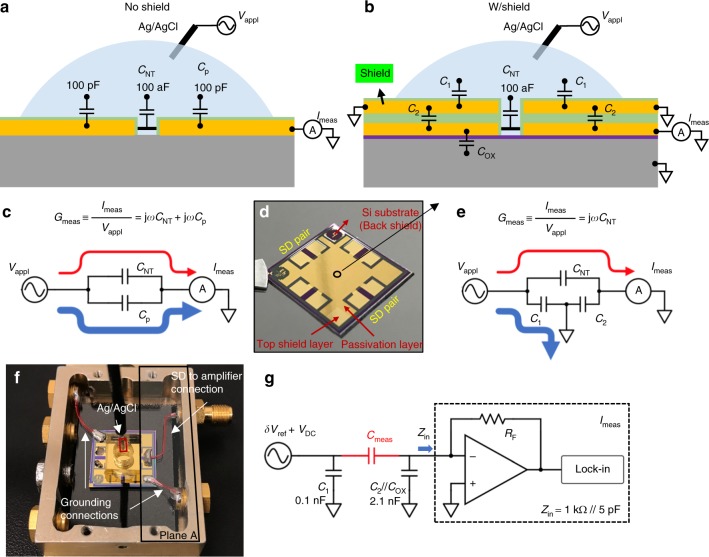
Fig. 1.
Liquid-gated nanotube devices with an integrated on-chip shield. a, c Schematic diagrams and corresponding circuits of a nanotube device without integrated shield, versus b, e with integrated shield. For non-shielding case, the measured current between the liquid and the contact electrodes contains parasitic current (blue arrow line in subfigure c) that is ~6 orders of magnitude larger than the current passing through the nanotube (red arrow line), which easily swamps the current signal of interest and make it too difficult to measure. For the shielding case, the parasitic current (blue arrow line in subfigure e) is directed to the ground instead of the current meter. d Optical image of a device chip. The source-drain electrodes are patterned underneath the shielding layer and form contact with nanotubes in the center of the chip. f Wire connections of a device sitting inside a Faraday box. Copper wires between the device and the SMA connectors are highlighted with red color. A PDMS chamber is placed on top of the device as a liquid reservoir. The Ag/AgCl reference electrode is brought in the reservoir by a coaxial cable. Plane A is covered with a grounded metal plate during the measurement to further eliminate the parasitic current. g Circuit model of the device and the measurement units. Currents that pass through the parasitic capacitances (C1, C2, and Cox) are directed to the ground. Currents that pass through the SWNT-electrolyte interface are input to the pre-amplifier and the lock-in amplifier, to characterize the corresponding capacitance Cmeas. The input impedance of the pre-amplifier is 1 kΩ // 5 pF

