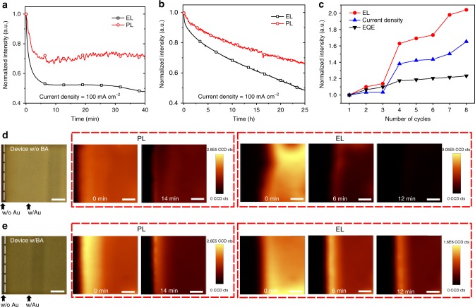
Fig. 2.
Optoelectronic characteristics of the aged devices. a EL and PL decay of the 3D PeLEDs without BA treatment at a constant current density of 100 mA cm−2. b EL and PL decay of the 3D PeLEDs with BA treatment at a constant current density of 100 mA cm−2. c Normalized device EL, current density and EQE under cyclic voltages between −1 and 2.5 V after aging test. The EL/current density/EQE show recovery. d Microscopy image and corresponding PL and EL intensity maps of device without BA treatment (scale bar, 70 μm), which show the degradation starts from the edge of Au electrode and the EL degrades faster than the PL. e Microscopy image and corresponding PL and EL intensity maps of device with BA treatment (scale bar, 70 μm), which show that the BA interfacial layer significantly suppresses the device degradation

