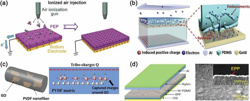
Figure 7.

(a) Fabrication illustration of the ionic molecule-injected fluorinated ethylene propylene (FEP) film and the final charge state of the FEP film for the contact-mode TEG. Reprinted with permission from [81]. Copyright 2014 John Wiley & Sons. (b) Schemes of electron drift in the G-TEG device (left) and electron escape from PDMS to Au (right). Reprinted with permission from [107]. Copyright 2018 American Chemical Society. (c) Schemes of PVDF/GO nanofibers presenting the dispersion of GO in the nanofiber (left) and stored charges on the surface of the GO sheet (right). Reprinted with permission from [108]. Copyright 2015 Springer Nature. (d) Device design of the as-fabricated TEG improved by the hole transport layer (left) and the top-view and cross-sectional SEM images of the hole transport layer, showing ethylene glycol (EG)-PEDOT:PSS (EPP) layer coated PDMS surface (right and inset). Reprinted with permission from [110]. Copyright 2016 American Chemical Society.
