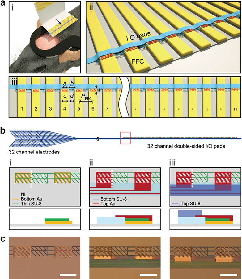
Figure 1. Overview of direct contact input/output (I/O) interface for syringe-injectable mesh electronics.
(a) Schematics illustrating the concept of direct contact I/O interface. (i) Mesh electronics (blue) implanted into the mouse brain (pink) with the I/O portion of the mesh ejected over and electrically-connected to the metal leads (gold) of a FFC, where the FFC is bonded to a head stage (black) glued to the mouse skull. (ii) Close-up view of the I/O interface indicated by the blue arrow in (i), where double-sided metal I/O pads (red) directly contact the FFC metal leads (gold), and electrically isolated parallel interconnect lines are indicated by the blue linear structure. (iii) Scalability of direct contact interface, where n indicates the number of I/O pads on the mesh probe that are contacted simultaneously to n metal leads on the FFC or other instrument interface. Here we focus on n = 32. The design parameters a, b, c, d, l and PFFC correspond to the width of I/O pad, the gap between neighboring I/O pads, the width of metal FFC leads, gap between neighboring metal FFC leads, the length of the I/O pad, and the pitch of the FFC, which is defined as PFFC = c + d = a + b, respectively. (b) Schematic of the 32-channel mesh electronics neural probe, highlighting (left) mesh structure with neural recording electrodes, (middle) parallel interconnects, and (right) corresponding double-sided I/O pads. Key fabrication steps of I/O pads are shown in close-up views from the red box: (i) Bottom Au pads (orange) are fabricated on Ni sacrificial layer (gray), with the thin SU-8 layer (green) patterned on top of and connecting between the bottom Au pads; (ii) bottom passivation layer of SU-8 (light blue) is patterned. Parallel metal interconnects are fabricated on this layer and connect to the top Au pads (dark red), which are fabricated on top of the bottom Au/thin SU-8; (iii) top passivation layer of SU-8 (darker blue) is fabricated to encapsulate the metal interconnects but leave the bottom/top (double-sided) I/O pads exposed. The bottom row of diagrams show corresponding side-view structures along the white vertical dashed lines in the top row. (c) Bright-field microscopy images of the fabrication steps corresponding to the schematics in (b) for design III discussed in text and Figure 2. Scale bars, 200 μm.

