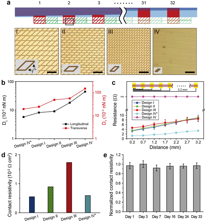
Figure 2. Designs and properties of direct contact I/O pads.
(a) Top, schematic of 32-channel direct contact I/O pads. Bottom, optical microscopy images of four I/O pad designs (designs I to IV) with different unit-cell sizes. Two different I/O pads are made for IV, where design IV* has the same in-plane geometry as design IV but the total thickness is halved (ca. 150 nm for design IV* vs. 300 nm for design IV). Scale bars, 200 μm. The insets show schematics of the corresponding unit cells. (b) Simulated bending stiffness for the longitudinal (DL, left y-axis) and transverse directions (DT, right y-axis) for the five I/O pad designs, I, II, III, IV and IV*. (c) Measured pairwise resistance values for the five I/O pad designs as a function of distance between two FFC leads, on which a continuous mesh I/O pad is mounted (top schematic). Error bars denote ±1-standard deviation (SD). (d) Contact resistivities are defined as contact resistance, Rc (1.16, 1.27, 2.02, and 0.34 Ω) derived from the extrapolated y-intercepts in (c), multiplied by ideal contact areas, Ac (0.004, 0.006, 0.008 and 0.012 cm2) based on the unit cells of designs I, II, III, and IV*. (e) Measured contact resistivity of design III over one month, normalized against the maximum value from the chronic measurements. A single-factor ANOVA test was used to determine if there was a significant change in the mean contact resistivity over time, which yields a p-value of 0.9142, suggesting that there is no statistically significant change in contact resistivity over at least one month. Error bars denote ±1 SD.

