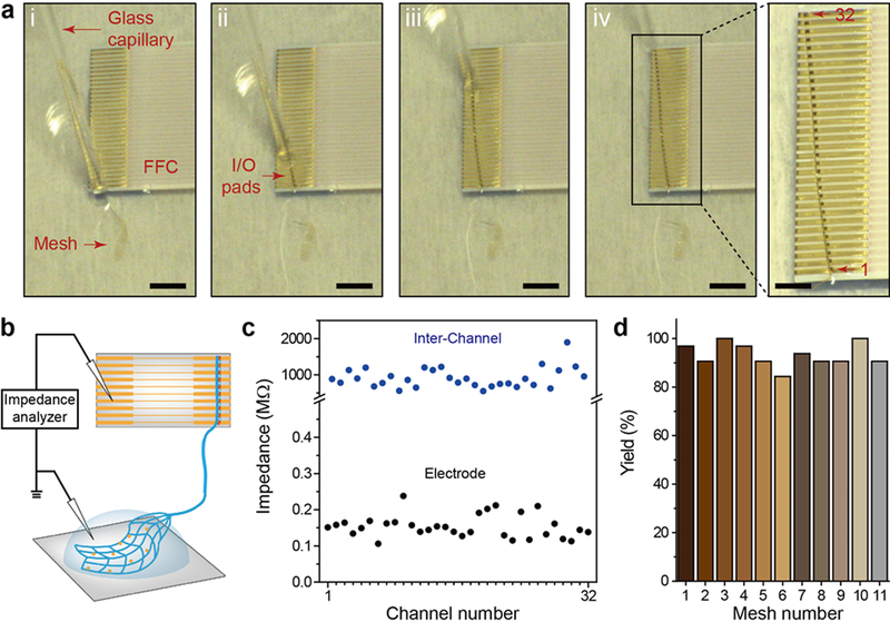
Figure 3. In-vitro demonstration and characterization of direct contact I/O interface.
(a) A series of optical microscopy images ((i) to (iv)) showing electrical connection of mesh I/O pads to the FFC via the direct contact I/O interface. Scale bars, 4 mm. Right, zoomed-in image of the black box in (iv), which shows 100% alignment of I/O pads with FFC metal leads (32 out of 32 channels). Scale bar, 2 mm. (b) Schematic of impedance measurement, where 1× phosphate-buffered saline (PBS) solution covers the recording electrode region of the mesh electronics to complete the circuit for impedance measurement. (c) Measured in-vitro electrode (black dots) and inter-channel (blue dots) impedance values at 1 kHz of a 32-channel mesh. (d) Yields of electrical connection of eleven 32-channel meshes with the direct contact I/O interfaces.

