Abstract
The fundamental absorption spectrum of a solid yields information about critical points in the optical density of states. This information can be used to adjust parameters of the band structure. Once the adjusted band structure is known, the optical properties and the density of states can be generated by numerical integration. We review in this paper the parametrization techniques used for obtaining band structures suitable for density of states calculations. The calculated optical constants are compared with experimental results. The energy derivative of these optical constants is discussed in connection with results of modulated reflectance measurements. It is also shown that information about density of empty states can be obtained from optical experiments involving excitation from deep core levels to the conduction band.
A detailed comparison of the calculated one-electron optical line shapes with experiment reveals deviations which can be interpreted as exciton effects. The accumulating experimental evidence pointing in this direction is reviewed together with the existing theory of these effects.
A number of simple models for the complicated interband density of states of an insulator have been proposed. We review in particular the Penn model, which can be used to account for response functions at zero frequency, and the parabolic model, which can be used to account for the dispersion of response functions in the immediate vicinity of the fundamental absorption edge.
Keywords: Critical points, density of states, dielectric constant, modulated reflectance, optical absorption
1. Optical Properties and One-Electron Density of States
The optical behavior of semiconductors and insulators in the near infrared, visible, and ultraviolet is determined by electronic interband transitions. An additional intraband or free electron contribution to the optical properties has to be considered for metals. We shall discuss here the relationship between the interband contribution and the density of states. The interband contribution to the imaginary part of the dielectric constant can be written as (in atomic units, ħ = m = 1, e = 1):
| (1) |
where ωef = ωe − ωf is the difference in energy between the empty bands (e) and the filled bands (f). The spin multiplicity must be included explicitly in eq (1). The oscillator strength tensor Fef is related to the matrix elements of p through Fef = 2 < f∣p∣e > < e∣p∣f > ωef−1. The Bloch functions are normalized over unit volume. Degenerate statistics has been assumed in eq (1) and spatial dispersion effects have been neglected.
It is customary to take the slowly varying oscillator strength out of the integral sign in eq (1) and thus write:.
| (2) |
where is an average oscillator strength and Nd the combined optical density of states.
Structure in ϵi(ω) (eq (1)) appears in the neighborhood of critical points, where ▽kωef = 0. Such critical points can be localized in a small region of k space or can extend over large portions of the Brillouin zone over which filled and empty bands are parallel (sometimes only nearly parallel). Once the critical points which correspond to observed optical structure are identified in terms of the band structure through various devious and sometimes dubious arguments, their energies can be used to adjust parameters of semiempirical band structure calculations.
Four different parametric techniques of calculating band structures have been used for this purpose: the empirical pseudopotential method (EPM) [1], the k · p method [2], the Fourier expansion technique (FE) [3], and the adjustable orthogonalized plane waves method (AOPW) [4].
Once reasonably reliable band structures are known it is important to calculate from them the imaginary part of the dielectric constant ϵi(ω) and to compare it with experimental results so as to confirm or disprove the initial tentative assignment of critical points and thus the accuracy of the band structures. Rich structure is obtained in both experimental and calculated spectra and hence a rather stringent test of the accuracy of the available theoretical band structure is in principle possible.
In order to calculate numerically the integral of eq (1) it is necessary to sample eigenvalues and eigenfunctions at a large number of points in the Brillouin zone. The amount of computer time required for solving the band structure problem with first-principles methods (OPW, APW, KKR) at a general point of the Brillouin zone makes such methods impractical for evaluating eq (1). The parametric methods (EPM, k · p, FE, but not AOPW) require only the diagonalization of a small matrix (typically 30 × 30) and hence it is possible to sample the band structure at about 1000 points with only a few hours of computer time. Cubic materials, in particular those with Td, O, and Oh point groups, are simple in this respect: symmetry reduces the sampling required for the evaluation of eq (1) to only 1/28 of the Brillouin zone. Hexagonal and tetragonal materials have relatively larger irreducible zones and hence a larger number of sampling points is necessary if the resolution of the calculation is not to suffer. Once the band structure problem has been solved for all points of a reasonably tight regular mesh, the bands and matrix elements at arbitrary points can be obtained by means of linear or quadratic interpolation.
The method of Gilat and coworkers [5] has become rather popular for the numerical evaluation of eq (1) [4,6]. In the case of a cubic material the Brillouin zone is divided into a cubic mesh and the band structure problem solved at the center of these cubes (sometimes a finer mesh is generated by quadratic interpolation from the coarser mesh [6]). Within each cube of the mesh the bands are linearily interpolated and approximated by their tangent planes. The areas of constant energy plane within each cube corresponding to a given ωef are added after multiplying them by the corresponding oscillator strength and thus the integral of eq (1) is obtained.
The real part of the dielectric constant ϵr can be obtained from ϵi by using the Kramers-Kronig relations. It is also possible to obtain ϵr and ϵi simultaneously by calculating the integral:
| (3) |
with η small and positive. For η → + o the imaginary part of eq (3) coincides with eq (1). Equation (3) can be evaluated with a Monte Carlo technique. Points are generated at random in k space within the Brillouin zone and the average value of the integrand for these points calculated. The process can be interrupted when reasonable convergence as a function of the number of random points is achieved [7,8].
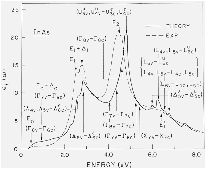
We show in figure 1 the results of a calculation of ϵi from the k · p band structure of InAs with the method of Gilat and Raubenheimer [6]. The band structure problem, including spin-orbit effects, was solved at about 200 points of the reduced zone (1/28 of the BZ). We have indicated in this figure the symmetry of the critical points (or of the approximate regions of space) where the structure in ϵi originates. The experimental ϵi spectrum, as obtained from the Kramers-Kronig analysis of the normal incidence reflectivity [9], is also shown. The agreement between calculated and experimental spectra is good, with regards to both position and strength of the observed structure, with the exception of the position of the E2 peak. This is to be attributed to an improper assignment of the E2 peak when the 6 adjustable band structure parameters were determined. The E2 peak had been attributed, following the tradition, to an X critical point while it is actually due to an extended region of k space centered around the U points [8]. It should be a simple matter to readjust the band structure parameters to lower the energy of the calculated E2 peak by about 0.5 eV; in view of the large amount of computer time required to recalculate the energy bands this has not been done. The structure calculated around 6 eV, due mostly to spin-orbit splitting of the L3 levels, has not yet been observed experimentally.
Figure 1.
Imaginary part of the dielectric constant of InAs as calculated from the k · p method (——) [6] and as determined experimentally (----) [9]. The group theoretical symmetry assignments were made with the help of the calculated isoenergy plots.
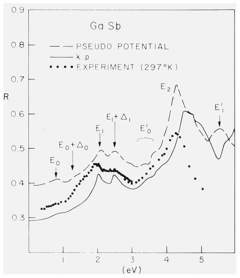
The conventional experimental determination of ϵi, from normal incidence reflection data [9] suffers from considerable inaccuracy: to the experimental error produced by possible improper surface treatment and contamination one has to add the uncertainty in the high-energy extrapolation of the experimental data required for the Kramers-Kronig analysis. Some of these difficulties are avoided by comparing the calculated reflectivity spectra (obtained from ϵ with Fresnel’s equation) with the experimental results. This is done in figure 2 for GaSb: the experimental data [10] have not been Kramers-Kronig analyzed because of the small range of the energy scale. Two calculated spectra have been plotted in this figure: one obtained from the k · p band structure [6] and the other obtained from a non-local pseudopotential calculation with 14 adjustable parameters [11]. The discrepancy between experimental and calculated curves at high energy, a common feature of many zincblende-type materials [12], has two origins: the measured reflectivity should be low because of increased diffuse reflectance at small wavelengths while the calculated one should be high because of the finite number of bands included in the calculation. In this region where ϵr − 1 is small, the contribution to ϵr of transitions not included should lower the calculated reflectivity.
Figure 2.
Reflectivity of GaSb calculated from the k · p [6] and from a pseudopotential band structure [11]. Also, experimental reflectivity [10].
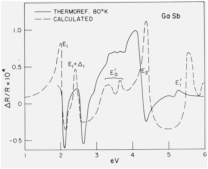
During the past few years a lot of activity has been devoted to the measurement and analysis of differential reflection spectra obtained with modulation techniques [13–15]. The wavelength (or photon energy) derivative spectra [14] should permit an accurate analysis of the line shapes of the spectra of figures 1 and 2. We show in figure 3 the temperature modulated reflection spectrum (thermoreflectance) of GaSb [15]: it has been shown that for the III – V materials [15] this spectrum is very similar to the photon energy derivative spectrum, difficult to obtain experimentally. The corresponding photon energy derivative spectrum obtained from the calculation of figure 2 is also shown in figure 3. The calculated and experimental shapes of the E1, E1 + Δ1 peaks show discrepancies of the type attributed in section 2 to exciton interaction. Derivative spectra for other germanium- and zincblende-type materials have been calculated by Walter and Cohen [12] and by Higginbotham [16].
Figure 3.
Measured thermoreflectance spectrum of GaSb [15] compared with the energy derivative of the spectrum of figure 2 [16].
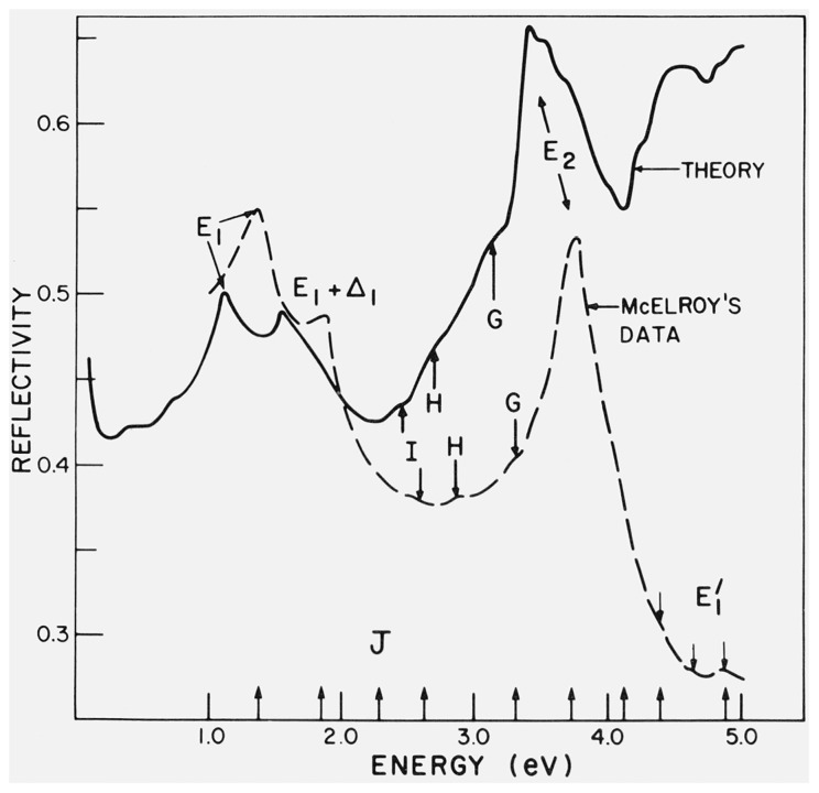
The methods to calculate band structures from first principles, without or with only a few adjustable parameters (one [17] or three [4]) have recently achieved considerable success. However the calculation of energy bands at one general point of the BZ requires a lot of time so as to make density of states calculations prohibitive. Moreover, the evaluation of the matrix elements required for eq (1) is difficult with first principles techniques. It is nevertheless possible to use first principles calculations at a few high-symmetry points of the Brillouin zone to adjust the parameters of semiempirical band structures from which the large number of sampling points required for the evaluation of eq (1) can be obtained with relative ease. The k · p technique has proved particularly useful in this respect [2,18,19]. Matrix elements of p can be easily evaluated from the eigenvectors in the k · p representation. Spin-orbit interaction can also be easily included. This k · p procedure has been applied to the relativistic OPW band structure calculated by Herman and Van Dyke for gray tin [19]. Figure 4 shows the reflectivity of gray tin calculated by this procedure with the method of Gilat and Raubenheimer together with experimental results [20]. Comparison with other experimental results for the germanium family suggests that the high-energy end of the measured spectrum is too low, probably due to surface imperfections in the delicate crystals, grown from mercury solution, which were used for this experiment.
Figure 4.
Reflectivity of gray tin calculated from a first principles OPW band structure fitted with the k · p method [19]. Also experimental results [20].
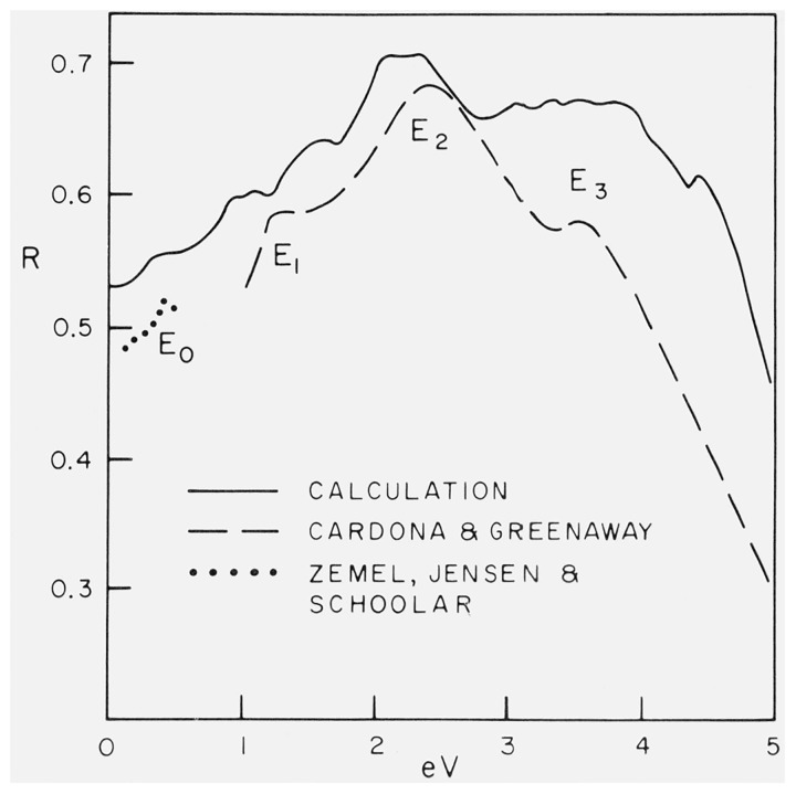
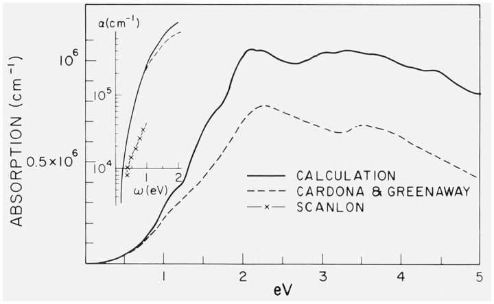
The k · p fitting procedure has also been applied to a first principles relativistic APW calculation of the band structure of PbTe by Buss and Parada [7]. Figure 5 shows the reflectivity of PbTe obtained by this method with a Monte Carlo sampling technique and figure 6 the absorption coefficient, both compared with experimental data [7,21,22]. In both cases the semiquantitative agreement between experimental and calculated data is remarkably good in view of the absence of the adjustable parameters. The calculated reflectivity is, at high energies, considerably higher than the experimental one, as discussed earlier for other materials. The E1 peak of the experimental reflectivity spectrum appears split in the calculated spectrum, possibly because of inaccuracies in the first-principles band structure. The calculated E1 structure appears due mostly to transitions along the Σ direction. The experimental E1 structure has been assigned [23] to the lowest gap along Σ. The calculated E2 peak corresponds to an extended region of the BZ without definite symmetry, as inferred from electroreference measurements [23].
Figure 5.
Reflectivity of PbTe calculated from the APW-k · p band structure [7], compared with experimental results [21].
Figure 6.
Absorption coefficient PbTe calculated from the APW-k · p band structure, compared with experimental results [21, 22].
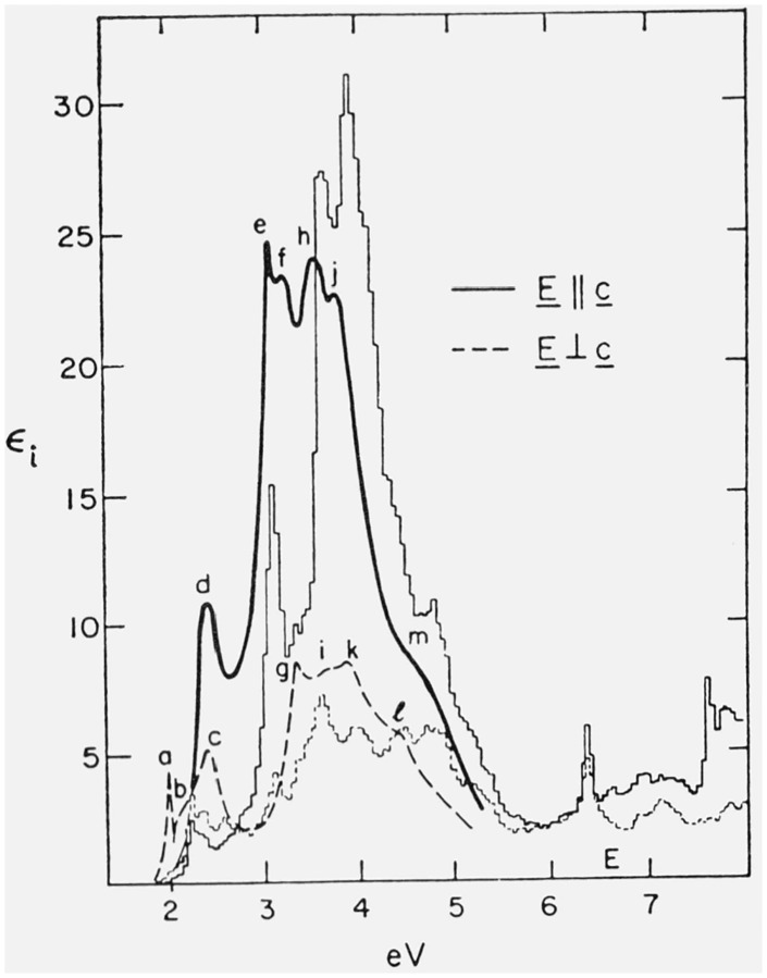
We have so far discussed optical constants for cubic materials. While calculations for materials with lower symmetry require more computer time, one has the extra reward of being able to predict the experimentally observed anisotropy. Figure 7 shows the two principal components of ϵi for trigonal Se as calculated by Sandrock [24] from the pseudopotential band structure. The similarity between calculated and experimental results [25], also shown in figure 7, is especially remarkable in view of the method used to determine the pseudopotential parameters: they were determined from the pseudopotential parameters required to fit the optical structure of ZnSe. Only a small adjustment was performed so as to bring the calculated fundamental gap (1.4 eV) into agreement with the experimental one (2.0 eV). The dielectric constant of antimony (trigonal) for the ordinary and the extraordinary ray has also been calculated by a similar procedure [26].
Figure 7.
Imaginary part of the dielectric constant of trigonal selenium for both principal directions of polarization of the electric field vector E as calculated from the pseudopotential band structure (histograms) [24] and as determined experimentally [25].
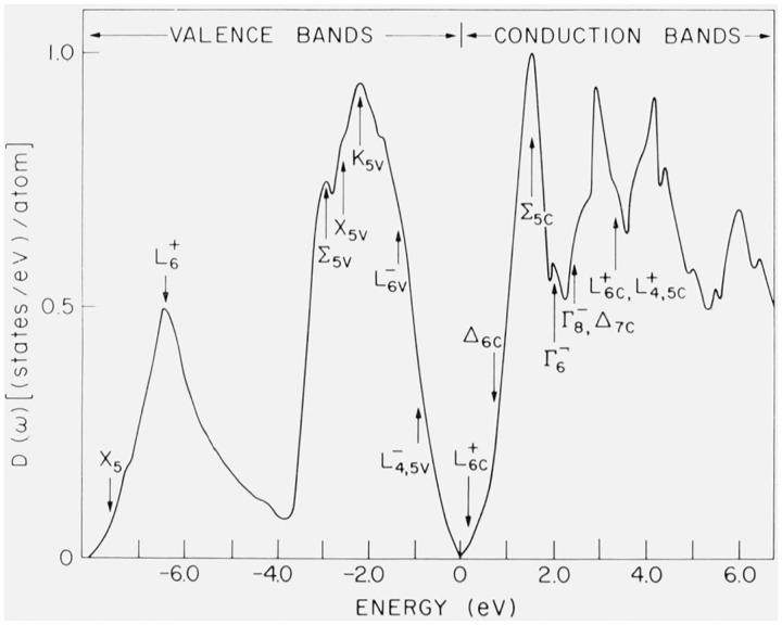
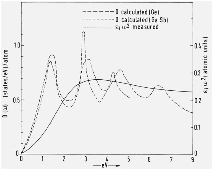
The reasonable agreement obtained between experimental and calculated optical constants suggests the use of the corresponding band structure to determine the individual density of states D(ω): the main work, that of diagonalizing the Hamiltonian at a large number of points, has already been done. The programs required to calculate individual density of states are very similar to those used for the evaluation of eq (1): ωef must be replaced by the single band energies and Fef must be removed. As an example we show in figure 8 the individual density of states of the 3 highest valence bands (six including spin) and the 3 lowest conduction bands of gray tin [19]. Direct information about the individual density of states can be obtained by a number of methods discussed in this conference. We mention, in particular, optical techniques involving transitions from deep core levels to the conduction band or from the valence band to temporarily empty core levels (soft x-ray emission) [27]. If the sometimes questionable assumption of constant matrix elements is made, the corresponding spectra represent the conduction (for absorption spectra) and the valence (for emission spectra) density of states because of the small width of the core bands. We show in figure 9 the density of states of the conduction band of Ge calculated by Herman, et al. [4] and the corresponding density of states for GaSb as obtained by the k · p method [6]. The densities of states for both materials are very similar because of the similarity of their band structures. We also show in figure 9 the quantity ϵiω2 obtained by Feuerbacher et al. [28] for Ge in the region of the M4,5 edge. The origin of energies has been shifted so as to make a comparison with the conduction density of states possible: ϵiω2 should be proportional to D(ω) under the assumption of constant matrix elements of p. While the rich structure of the calculated density of states is not seen in the ϵiω2 curve, this curve is reproduced quite well if the density of states is broadened so as to remove the fine structure. The required lifetime broadening of about 1 eV is not unreasonable for the M4,5 transitions. Using eq (2) with Nd replaced by the conduction density of states we obtain an average oscillator strength at the maximum of ϵiω2F = 0.15. This oscillator strength corresponds to the 20 4d electrons per unit cell and hence it should be divided by 20 to obtain the average oscillator strength per d-band. If one reasons that the transitions from 10 of the 20 d bands to a given conduction band are forbidden because of the spin flip involved while transitions from 5 of these 10 bands are forbidden or nearly forbidden by parity, one finds for the average oscillator strength of each one of the 5 allowed bands , which corresponds to a matrix element of p = 0.13 (in atomic units): this value is quite reasonable in view of the fact that the typical valence-conduction matrix element is 0.6. The small value of this matrix element explains why the d core electrons are negligible in the k · p analysis of the valence and conduction masses.
Figure 8.
Individual density of states for gray tin, obtained from the OPW-k · p band structure [19]. The top of the valence band is at 0 eV. The lowest valence band is not included.
Figure 9.
Conduction density of states calculate for Ge [4] and for GaSb [6] together with the function ϵiω2 obtained from experimental data in the vacuum uv [28] (the horizontal scale for the ϵiω2 curve has been shifted by 29.5 eV).
2. Exciton Effects
We have devoted section 1 to a comparison of experimental optical spectra with calculations based on the one-electron band structure. Exciton effects, i.e. the final state Coulomb interaction between the excited electron and the hole left behind, are known to modify substantially the fundamental edge of semiconductors and insulators [29]. Exciton-modified interband spectra seem also to occur in metals at interband edges which have the final state on the Fermi surface [30]. Experimental evidence for these effects is reported at this conference in the paper by Kunz et al.
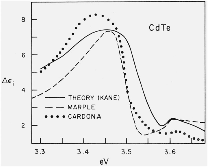
We shall now discuss the question of exciton effects above the fundamental edge of insulators and semiconductors with special emphasis on the zincblende family. As mentioned in section 1 the gross features of these spectra are explained by the one-electron theory. The exciton interaction is responsible, at most, for small details concerning the observed line shapes. It is generally accepted [31,32] that the exciton interaction suppresses structure in the neighborhood of M3 critical points: the Coulomb attraction with negative reduced masses is equivalent to a repulsion with positive masses. Such a repulsion smooths out critical point structure: no M3 critical point has been conclusively identified in the experimental spectra. The E1 and E1 + Δ1 critical points of figures 1 – 3 are of the M1 variety. Hence the line shape of the corresponding ϵi spectrum should be characterized by a steep low-energy side and a broader high-energy side. Figure 10 shows the shape of the E1 peak observed at low temperature by Marple and Ehrenreich [33] and by Cardona [34]. In order to avoid effects due to the overlap of the E1 and the E1 + Δ1 peaks it has been assumed that they have exactly the same shape but shifted by 0.55 eV. The contribution of only E1 has been extracted from the measured ϵi spectrum and displayed in figure 10. It is clear from this figure that the E1 peak is steeper at high energies than at low energies, against the expectations for an M1 peak. Also in figure 10 we show the results of a calculation by Kane [32] of the effect of Coulomb interaction on the E1 line shape for CdTe, using the effective mass approximation. The solution of the effective mass Hamiltonian with non-positive-definite mass is made easier by the fact that the negative mass (along the Λ direction) has a magnitude much larger (about ten times) than the two equal positive masses. It is possible to use the adiabatic approximation [31], i.e., to solve the two-dimensional hydrogen atom problem with the third coordinate as a parameter and then solve the adiabatic equation for the third coordinate. The agreement between the calculated and the experimental line shapes of figure 10 is excellent.
Figure 10.
Contribution of the E1 gap to ϵi in CdTe as measured at low temperatures by Marple and Ehrenreich [33] and by Cardona [34]. Also calculation by Kane [32] using the adiabatic approximation.
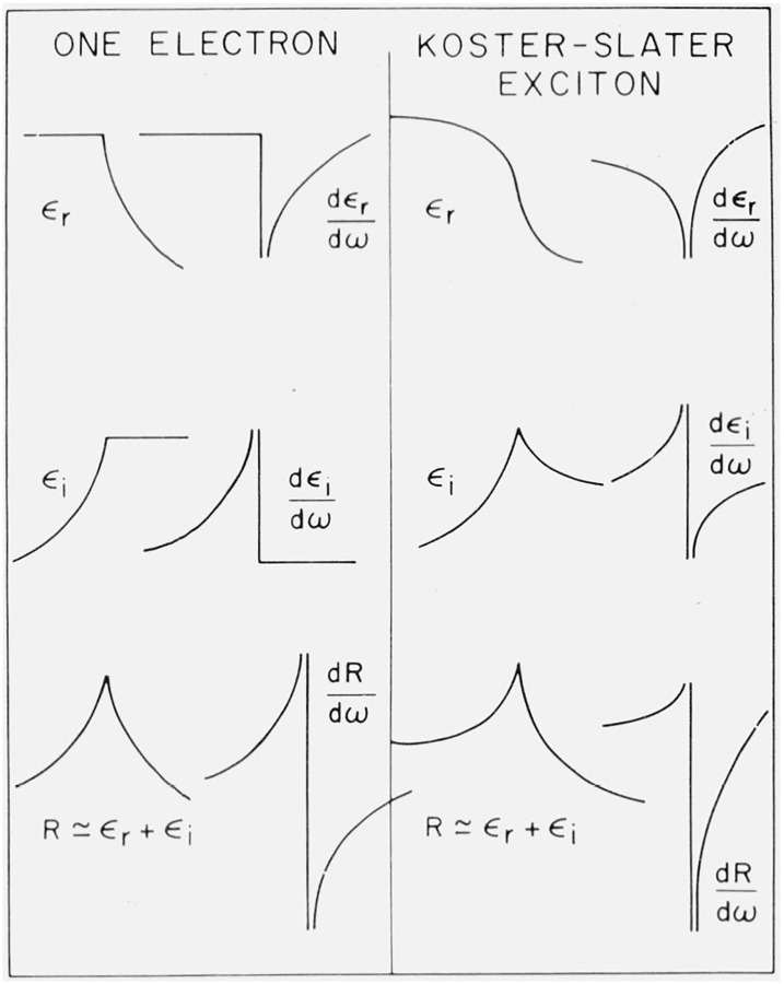
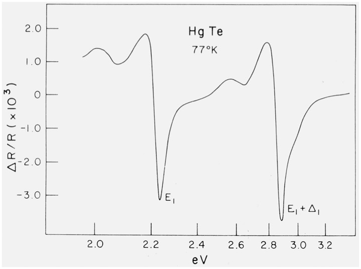
Attempts have been made to calculate the dielectric constant including exciton interactions at an arbitrary point of k space, independently of the stringent restrictions of the effective mass approximation [35,36]. Such calculation is possible if one truncates the Coulomb interaction between electron and hole Wannier packets to extend to a finite number of neighboring cells. The extreme and simplest case of a δ-function (Koster-Slater) interaction can be solved by hand [31,35] and gives around an M1 critical point the shapes of ϵr and ϵi shown in figure 11: for an Mi critical point the Koster-Slater interaction mixes the Mi one-electron line shape with the Mi+1. The high energy side of the ϵi peak becomes steeper, in agreement with figure 10. The line shape observed for the E1 − E1 + Δ1 peaks in the reflectivity spectrum is composed almost additively of the ϵi and ϵr line shape: at the energies of these peaks dR/dϵi and dR/dϵr are almost equal. We also show in figure 11 the line shapes expected for the reflectivity spectra of the E1− E1 + Δ1 peaks and for the corresponding differential spectra (dR/dω). We show in figure 12 the photon energy derivative spectrum of these peaks in HgTe [37]: the observed line shapes disagree with those expected from the one-electron theory (equal positive and negative peaks) but agree with those predicted in the presence of a Koster-Slater interaction (fig. 11). Similar results have been found for other zincblende-type materials [37].
Figure 11.
Modification in ϵr and ϵi introduced by the Koster-Slater exciton interaction in the neighborhood of an M1 critical point. Also, effect on the reflectivity under the assumption of an equal contribution of Δϵr and Δϵi to the reflectivity line shape.
Figure 12.
Photon energy derivative spectrum of the reflectivity of HgTe in the neighborhood of the E1 and E1 + Δ1 structure [37].
3. Simplified Models for the Density of States
As seen in section 1 the optical density of states, and thus the dielectric constant, is a complicated function of frequency and its calculation requires lengthy numerical computation. For some purposes, however, it can be approximated by simple functions. In the vicinity of a critical point of the Mi variety, for instance, the singular behavior of the dielectric constant can be approximated by:
| (4) |
if exciton effects are neglected. Exciton interaction can be included, within the Koster-Slater model, by multiplying eq (4) by a phase factor ϵiϕ with ϕ small and positive.
As shown in figure 1, ϵi for the zincblende-type materials has a strong peak (E2) in the neighborhood of which most of the optical density of states is concentrated. The corresponding transitions occur over a large region of the BZ, close to its boundaries. In order to represent this fact, Penn [38] suggested the model of a non-physical spherical BZ with an isotropic gap at its boundaries. The complex energy bands of the material are then replaced by those of a free electron with an isotropic gas ωg at the boundary of a spherical BZ. This gap should occur in the vicinity of the E2 optical structure. While this model represents rather poorly the rich structure of ϵi (fig. 1), it is expected that it should give a good picture of ϵr at zero frequency. The reshuffling of density of states involved in the case of the isotropic model should not affect ϵr(ω = o) very much because of the large energy denominators which appear in eq (3) for ω = o: the lowest gap ωo, usually much smaller than ωg, accounts only for a very small fraction of the optical density of states. Penn obtained with this model the static dielectric constant for a finite wavevector q. The result can be approximated by the analytic expression [38]:
| (5) |
with
In eq (5) ωp is the plasma frequency obtained for the density of valence electrons and ωF and kF the corresponding free electron Fermi energy and wave number. The dimensionless quantity is usually close to one.
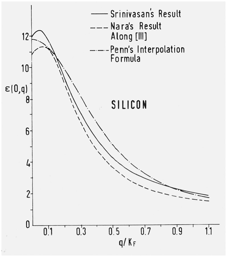
Figure 13 shows eq (5) for Si compared with the exact results of the Penn model [39]. These results are obviously independent of the direction of q. A small dependence on this direction is found from a complete pseudopotential calculation by Nara [40] (see also fig. 13). The function ϵ(o,q) is of interest for the treatment of dielectric screening.
Figure 13.
Static dielectric constant ϵ(o, q) obtained by Srinivasan [39] for Si with the Penn model compared with the interpolation formula of eq (5) and with the results of a pseudopotential calculation by Nara [40] for q along (111).
Equation (5) yields for q = o the electronic contribution to the static dielectric constant:
| (6) |
The experimental values of ϵo agree reasonably well with the results of eq (6) using for ωg the energy of the E2 peak [34]. Equation 6 has gained recent interest as the basis of Phillips and Van Vechten’s theory of covalent bonding [41,42,43]. These authors use eq (6) and the experimental values of ϵo to define the average gap ωg. With this gap and the corresponding gap of the isoelectronic group IV material they can interpret a wide range of properties such as crystal structure [42], binding energy [43], energies of interband critical points [41], non-linear susceptibilities [44], etc. As an example we discuss the hydrostatic pressure (i.e. volume) dependence of ϵo for germanium and silicon. According to Van Vechten [41], ωg for C, Ge, Si, and α − Sn is proportional to (ao)−2.5 where ao is the lattice constant. If one makes the assumption that this law gives also the change in ωg with lattice constant for a given material when hydrostatic stress is applied one can calculate the volume dependence of ϵo [41]. Neglecting the one in eq (6), a valid approximation for Ge and Si, one finds:
| (7) |
Equation (7) explains the sign and the small magnitude observed for (1/ϵo)(dϵo/dV). The experimental values of this quantity are 1.0 for Ge and 0.6 for Si [41,45].
According to eq (6) the average gap ωg determines the electronic dielectric constant for ω = o. As the lowest gap ωo is approached (ωo ⪡ ωg usually), ϵr exhibits strong dispersion. This dispersion is due, in the spirit of eq (3), to the density of states in the vicinity of ωo. For the purpose of calculating the dispersion of ϵr immediately below ωo, the density of states can be approximated by that of parabolic bands with a reduced mass equal to the reduced mass μ at ωo. These bands are assumed to extend to infinity in k space: the unphysical contribution to ϵr for ∣ k ∣→ ∞ should be small for ω ⩽ ωo, because of the large energy denominators of eq (3). We thus obtain for a cubic material the following contribution of the ωo gap to the scalar dielectric constant below ωo (under the assumption of a constant matrix element of p equal to P) [46]:
| (8) |
with
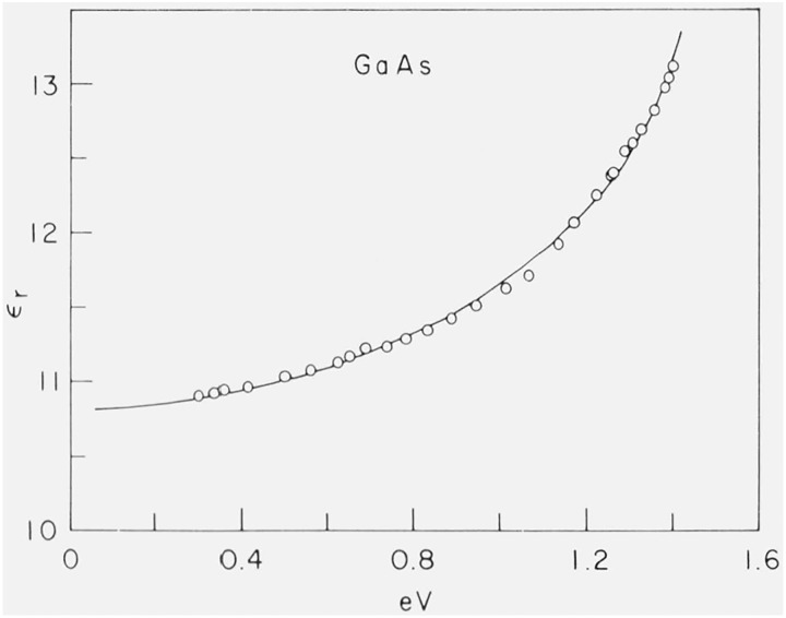
Equation (8) represents quite well the behavior of ϵr immediately below ωo for the lead chalcogenides [47] and a number of other semiconductors [48]. As an example we show in figure 14 the observed dispersion of ϵr below ωo at room temperature [49] together with a fit based on eq (8) [48]. For the sake of completeness we have included in the fitting equations not only the effect of ωo (Eo) but also that of its spin-orbit-split mate Eo +Δo (also represented by an expression similar to eq (8)), the dispersion due to the E1 and E1 +Δ1 gaps, and that due to the main ωg gap assuming ωg ≡ E2. Thus the fitting equation with three adjustable parameters , , is [48]:
| (9) |
where:
The fitting values of (6.602) and (2.791) are in qualitative agreement with those calculated from the band parameters [48].
Figure 14.
Experimental results for ϵr in GaAs below the fundamental edge at room temperature [49] (circles) and fitted curve based on a model density of states.
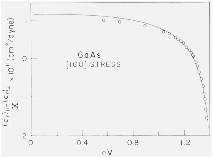
The parabolic model density of states can also be used to interpret the strong dispersion in the piezobirefringence observed near the lowest direct gap of Ge, GaAs [48], and other III – V semiconductors [50,51]: uniaxial stress splits the top valence band state (Γ8) and a birefringence in the contribution of Eo to ϵr results because of the selection rules for transitions from the split bands. The main contribution to this piezobirefringence is expected to be proportional to f′(x), which diverges like (ω − ωo)−1/2 for ω → ωo Such behavior can be seen in the experimental results (circles) of figure 15 obtained for GaAs at room temperature. Included in this figure is the corresponding fit based on the model of eq (9) [48].
Figugre 15.
Piezobirefringence in GaAs for an extensive stress along (100) (room temperature). The circles are experimental points. The solid line is a fit based on the model of eq (5) [48].
The long wavelength, non-dispersive contribution to the piezobirefringence of figure 15 can be interpreted, at least qualitatively, in terms of the Penn model of eqs (6) and (7). Equation (7) yields two contributions to the change in ϵr one due to the change in plasma frequency (i.e. carrier density) with stress and the other due to the change in the isotropic gap. The first contribution should not exist for a pure shear stress. For a hydrostatic stress the second contribution can be written in tensor form as:
| (10) |
where e is the strain tensor. We postulate that eq (8) remains valid for pure sheer stress. This crude generalization has a clear physical meaning in terms of the Penn model. The spherical BZ becomes ellipsoidal under a sheer stress and the energy gap at an arbitrary point of the BZ boundary kF becomes anisotropic. The gap at kF is assumed to become larger as kF becomes larger (kF is the distance between atomic planes perpendicular to kF). Equation (8) gives the right sign for the long wavelength contribution to the piezobirefringence of figure 15 but a magnitude about five times larger. The agreement becomes better if the contribution of the Eo edge to the long wavelength piezobirefringence, of opposite sign to that predicted by eq (10), is subtracted from the experimental results.
4. Third Order Susceptibility and Model Density of States
It has been recently suggested [52] that the third order susceptibility of Ge, Si, and GaAs at long wavelengths is related to the Franz-Keldysh effect (i.e. the intraband coupling by the field) of interband critical points [53]. We discuss now the Franz-Keldysh contribution of the ωg, Eo, and E1 gaps to .
4.1. Average Gapωg
In the spirit of Penn’s model [38] we represent the long-wavelength dielectric constant by eq (6) with . The corresponding imaginary part of the dielectric constant is, for ω > ωg [47]:
with
| (11) |
The Franz-Keldysh effect for the one-dimensional absorption edge of eq (11) can be expressed in terms of the Airy functions Ai and Bi [54]. One must mention, however, that the isotropic gap problem in the presence of an electric field would only be completely equivalent to the one-dimensional problem if the field experienced by every electron were along the direction of the corresponding k. The fact that the field is the same for all electrons, regardless of k, can be taken into account by using an average field:
| (12) |
where β is the angle between k and . The long-wavelength expression for thus is [54]:
| (13) |
where the one-dimensional electro-optic function G1 (η) is given by [54]:
| (14) |
In eq (14) H (η) is the unit step function and μ the reduced mass of the Penn model, given by μ = ωg(2kF)−2. The Fermi momentum of the valence electrons is related to the plasma frequency ωp through kF3 = (1/2)πωp2.
The limit for in eq (14) is easily found using the asymptotic expansions of Ai (η) and Bi (η) for η → + ∞ [55]. By subsequently performing the limit for ω → 0 one finds:
| (15) |
Or, for ease of evaluation, with in e.s.u., and the energies in eV:
| (16) |
We list in table I the values of ωg, ωp and ϵo − 1 for Ge, Si and GaAs. The values of calculated with eq (16) are then listed in table II. This table shows agreement in sign and magnitude between the values of predicted from ωg and the experimental ones. An increase in the polarizability with field () is to be expected for the Franz-Keldysh effect since the intraband coupling by the electric field produces a decrease in the energy gap.
Table I.
Values of the parameters required for the evaluation of the Franz-Keldysh contributions to . Frequencies in eV, ao in Bohr radii, μo in units of the free electron mass. p2 has been taken equal to 0.4 for all materials.
| Ge | Si | GaAs | |
|---|---|---|---|
| ωg | 4.3 | 4.8 | 5.2 |
| ωp | 15.5 | 17.35 | 15.5 |
| ϵ0 – 1 | 11 | 15 | 10 |
| μ0 | 0.03 | 0.04 | 0.05 |
| ω0 | 0.9 | 4 | 1.5 |
| a0 | 10.7 | 10.3 | 10.7 |
| ω1 | 2.2 | 3.3 | 3.0 |
Table II.
Contribution of the various Franz-Keldysh effects discussed here to and. In units of 10−10 e.s.u. Also, experimental values of the bound carrier contributions to and .
| Eg contribution | E0 contribution | E1 contribution | Experilenl57 | |
|---|---|---|---|---|
| 0.26 | 0.67 | 0.20 | 1.0 | |
| 0.26 | 0.67 | 0.26 | 1.5 | |
| 0.22 | 0.00 | 0.27 | 0.06 | |
| 0.22 | 0.00 | 0.36 | 0.08 | |
| 0.12 | 0.087 | 0.045 | 0.12 | |
| 0.12 | 0.087 | 0.060 | 0.10 |
We shall consider now the contribution to of the interband coupling by the electric field across the isotropic gap ωg. This coupling produces an increase in energy gap, and thus its contribution to is negative. This contribution to is readily found from eq (6):
| (17) |
In eq (17) we have made use of the second-order perturbation expression:
| (18) |
Equation (18) is in agreement with the results of ref. [44]. Comparison of this equation with eq (15) shows that the magnitude of the interband contribution to differs from that of the intraband contribution by a factor of order ωg2 (ωg in atomic units). It is therefore almost two orders of magnitude smaller and hence negligible.
4.2. Lowest Gap Eo
We use for the contribution of an isotropic Mo critical point to the real part of the dielectric constant the result of eq (8). A calculation similar to that performed above yields for an Mo critical point the following Franz-Keldysh contribution to [52]:
| (19) |
or, transforming to e.s.u. and ωo to eV (P2 and μo are left in atomic units for ease of computation):
| (20) |
We have included in eqs (19) and (20) the first term in the dispersion of ϵr since it may be possible to observe it experimentally in small band gap materials. This dispersion is given exactly by the function:
| (21) |
Equation (21) is not immediately valid for the Eo edge because of the degeneracy of the valence band. However, one can apply it to the Eo edge if one neglects the field coupling between degenerate valence bands and uses appropriate average values of P2 and μo. Each one of the three valence bands can be assumed to have a mass equal to three times the conduction band mass and a corresponding matrix element equal to [48]. Hence eq (20) must be used with the matrix element P2 and if the three valence bands are to be included. The spin-orbit splitting Δo of the valence band is taken into account, if Δo ⪡ Eo, by replacing ωo by its average value . Since P2 is almost the same for all materials of the germanium family, we can replace it by a typical value ≈ 0.4 (in atomic units). The values of μo and for Ge, Si and GaAs are listed in table I. Using these numbers, eq (20) yields the values of (ω = 0) listed in table II. While this contribution is zero for Si and is not excessive in GaAs (it may, therefore, be assumed as included in the average gap calculation given above), it is dominant in Ge. In first approximation it may be added to the average gap calculation: excellent agreement with the experimental results is then found.
For InAs, with ωo = 0.5 eV and μ = 0.02, we find from eq (20) (ω = 0) = 7 · 10−10, which is of the order of the free-carrier contribution for the samples with the lowest electron concentrations measured (N = 2 · 1016 cm−3) [57]. This is contrary to the statement found in the literature that for these carrier concentrations in InAs dominated by the free-carrier contribution [56,57,58].
The interband contribution of Eo to for ω = 0 is easily obtained from the expression (see eq (8)):
| (22) |
If one assumes that the repulsion produced by the field affects μo in the manner predicted by the k · p expression with constant matrix elements of p(μo ∝ ωg), the corresponding interband contribution to vanishes. If, on the other hand, one assumes μo to be field independent one also finds a negative contribution to about two orders of magnitude smaller than the Franz-Keldysh contribution, and hence negligible.
4.3. E1 Critical Points
The E1 optical structure is usually attributed to M1 critical points along the {111} directions. While M1 critical points are known to yield no contribution to [52], there are Mo critical points of the same symmetry slightly below the M1 critical points. This combination of Mo and M1 critical points with a very large longitudinal mass, can actually be approximated by two-dimensional minima [48]. The contribution of one of these two-dimensional minima to the long-wavelength dielectric constant is (we assume four, and not eight equivalent {111} directions):
| (23) |
where ao is the lattice constant and P2 the appropriate square matrix element. We have tried to calculate the Franz-Keldysh contribution to two-dimensional critical points in a way similar to that used above, but we have run into difficulties when evaluating the limits of the two-dimensional electro-optic functions for η → + ∞. In view of this we have instead evaluated the effect of the three-dimensional Mo critical points, with the longitudinal effective mass replaced by the value required to give at long wavelengths a contribution to ϵr equal to that in eq (23).
Under these conditions, and because of the large longitudinal mass, only fields transverse to the critical point axis contribute to . When summing the contributions of the four equivalent valleys, it is found that the effect becomes anisotropic: the ratio of the third order susceptibility for along {111} , to that for along {100} is 4/3. This argument is independent of the specific model chosen for the {111} transitions, provided μ∣∣ ⪢ μ⊥. It gives the type of anisotropy observed for Ge and Si, but not for GaAs [57]. The Franz-Keldysh contribution of E1 to as found by the procedure sketched above, is:
| (24) |
or, with ω1 in eV and in e.s.u.:
| (25) |
(ao in Bohr radii and P2 in atomic units.)
The matrix element P should have approximately the same value as for the Eo gap. In order to take care of the spin-orbit splitting Δ1 of E1 we substitute ω1 by E1 + Δ1/2. The approximate values of ao, and ω1 for Ge, Si and GaAs are listed in table I. The values calculated for the Franz-Keldysh contribution to E1 to and are listed in table II. While the calculated anisotropy has, for Ge and Si, the sign observed experimentally, its magnitude is far too small to explain the experimental anisotropy, especially after the Eo and the Eg contributions are added. There is a possibility that the E1 contribution of eq (25) may have been underestimated. Exciton quenching effects [59,60], not included in our calculation, may increase this contribution.
We cannot offer even a qualitative explanation of the sign of the χ(3) anisotropy observed for GaAs. It would be interesting to determine, through measurements of other III – V or II– VI compounds, whether it is connected with the lack of inversion symmetry in these materials.
The interband contribution of the E1 edges can be evaluated in a manner analogous to that used for the Eo and the ωg gaps. We also find that this contribution is negative and, typically, two orders of magnitude below the Franz-Keldysh contribution.
5. Acknowledgments
I am indebted to Drs. Buss, Kane, Phillips, Van Vechten, and Aspnes for sending preprints of their work, prior to publication and to the staff of DESY for their hospitality.
Footnotes
An invited paper presented at the 3d Materials Research Symposium, Electronic Density of Stairs. November 3–6, 1969, Gaithersburg, Md.
Supported by the National Science Foundation and the Army Research Office, Durham.
John Simon Guggenheim Foundation Fellow.
6. References
- [1].Cohen M. L., and Bergstresser T. K., Phys. Rev. 141, 789 (1966). [Google Scholar]
- [2].Cardona M., and Pollak F. H., Phys. Rev. 142, 530 (1966). [Google Scholar]
- [3].Dresselhaus G., and Dresselhaus M. S., Phys. Rev. 160, 649 (1967). [Google Scholar]
- [4].Herman F., Kortum R. L., Kuglin C. D., and Shay J. L., in “II – VI Semiconducting Compounds,” Thomas D. G., ed., (W. A. Benjamin, New York, 1967), p. 503. [Google Scholar]
- [5].Gilat G., and Dolling G., Phys. Letters 8, 304 (1964); [Google Scholar]; Gilat G., and Raubenheimer L. J., Phys. Rev. 144, 390 (1966). [Google Scholar]
- [6].Higginbotham C. W., Pollak F. H., and Cardona M., Proceedings of the IX International Conference on the Physics of Semiconductors, Moscow 1968 (Publishing House Nauka, Leningrad, 1968) p. 57. [Google Scholar]
- [7].Buss D. D., and Parada N. J., private communication; see also article by D. D. Buss and V. E. Shirf in these proceedings.
- [8].Kane E. O., Phys. Rev. 146, 558 (1966). [Google Scholar]
- [9].Philipp H. R., and Ehrenreich H., Phys. Rev. 129, 1550 (1963). [Google Scholar]
- [10].Cardona M., Physik Z. 161, 99 (1961).
- [11].Zhang H. L, and Callaway J., Phys. Rev. 181, 1163 (1969). [Google Scholar]
- [12].Walter J. P., and Cohen M. L., Phys. Rev., to be published. [Google Scholar]
- [13].Seraphin B. O., and Bottka N., Phys. Rev. 145, 628 (1966). [Google Scholar]
- [14].Shaklee K. L., Rowe J. E., and Cardona M., Phys. Rev. 174, 828 (1968). [Google Scholar]
- [15].Matatagui E., Thompson A. G., and Cardona M., Phys. Rev. 176, 950 (1968). [Google Scholar]
- [16].Higginbotham C. W.,ph. D. Thesis, Brown University, 1969. [Google Scholar]
- [17].Eckelt P., Madelung O., and Treusch J., Phys. Rev. Letters 18, 656 (1967). [Google Scholar]
- [18].Brinkman W., and Goodman B., Phys. Rev. 149, 597 (1966). [Google Scholar]
- [19].Pollak F. H., Cardona M., Higginbotham C. W., Herman F., and Van Dyke J. P., Phys. Rev., to be published. [Google Scholar]
- [20].McElroy P.,ph. D. Thesis, Harvard University, 1968. [Google Scholar]
- [21].Cardona M., and Greenaway D. L., Phys. Rev. 133, A1685 (1964). [Google Scholar]
- [22].Scanlon W. W., J. Phys. Chem. Solids 8, 423 (1959). [Google Scholar]
- [23].Aspnes D. E., and Cardona M., Phys. Rev. 173, 714 (1968). [Google Scholar]
- [24].Sandrock R., Phys. Rev. 169, 642 (1968). [Google Scholar]
- [25].Tutihasi S., and Chen I., Phys. Rev. 158, 623 (1967). [Google Scholar]
- [26].Lin P. J., and Phillips J. C., Phys. Rev. 147, 469 (1966). [Google Scholar]
- [27].Wiech G., in “Soft X-Ray Spectra,” Fabian D. J., ed., (Academic Press, New York, 1968) p. 59. [Google Scholar]
- [28].Feuerbacher B., Skibowski M., Godwin R. P., and Sasaki T., JOSA 58, 1434 (1968). [DOI] [PubMed] [Google Scholar]
- [29].See for instance Knox R. S., “Theory of Excitons,” (Academic Press, N.Y., 1963). [Google Scholar]
- [30].Mahan G. D., Phys. Rev. Letters 18, 448 (1967). [Google Scholar]
- [31].Velicky B., and Sak J., Phys. Status Solidi 16, 147 (1966). [Google Scholar]
- [32].Kane E. O., Phys. Rev. 180, 852 (1969). [Google Scholar]
- [33].Marple D. T. F., and Ehrenreich H., Phys. Rev. Letters 8, 87 (1962). [Google Scholar]
- [34].Cardona M., J. Appl. Phys. 36, 2181 (1965). [Google Scholar]
- [35].Inoue M., Okazaki M., Toyozawa Y., Inui T., and Nanamura E., Proc. Phys. Soc. Japan 21, 1850 (1966). [Google Scholar]
- [36].Hermanson J., Phys. Rev. 150, 660 (1966). [Google Scholar]
- [37].Shaklee K. L.,ph. D. Thesis, Brown University, 1969. [Google Scholar]
- [38].Penn D., Phys. Rev. 128, 2093 (1962). [Google Scholar]
- [39].Srinivasan G., Phys. Rev. 178, 1244 (1969). [Google Scholar]
- [40].Nara H., J. Phys. Soc. Japan 20, 778 (1965). [Google Scholar]
- [41].Van Vechten J. A., Phys. Rev. 182, 891 (1969). [Google Scholar]; In this reference a correction factor of the order of unity is added to eq (6) so as to take the polarizability of the core d electrons into account.
- [42].Phillips J. C., Phys. Rev. Letters 20, 550 (1968). [Google Scholar]
- [43].Phillips J. C., Covalent Bonding in Molecules and Solids (University of Chicago Press, Chicago: ) to be published. [Google Scholar]
- [44].Phillips J. C., and Van Vechten J. A., Phys. Rev. 183, 709 (1969); [Google Scholar]; Levine B. F., Phys. Rev. Letters 22, 787 (1968). [Google Scholar]
- [45].Cardona M., Paul W., and Brooks H., J. Phys. Chem. Solids 8, 204 (1959). [Google Scholar]
- [46].Korovin L. I., Soviet Phys. Solid State 1, 1202 (1959). [Google Scholar]
- [47].Cardona M. in “High Energy Physics, Nuclear Physics, and Solid State Physics,” Saavedra I., ed., (W. A. Benjamin, New York, 1968). [Google Scholar]
- [48].Higginbotham C. W., Cardona M., and Pollak F. H., Phys. Rev. 184, 821 (1969). [Google Scholar]
- [49].De Meis W. M., Technical Report No. HP-15 (ARPA-16), Harvard University (1965). [Google Scholar]
- [50].Shileika A. Yu., Cardona M., and Pollak F. H., Solid State Communications 7, 1113 (1969). [Google Scholar]
- [51].Yu P. Y., to be published.
- [52].Van Vechten J. A., and Aspnes D. E., Phys. Letters, in press.
- [53].Aronov A. G., and Pikus G. E., Proceedings of the IX International Conference on the Physics of Semiconductors, Moscow, 1968, (Publishing House Nauka, Leningrad, 1968), p. 390. [Google Scholar]
- [54].Cardona M., “Modulation Spectroscopy,” Seitz F., Turnbull D., and Ehrenreich H., eds., (Academic Press Inc., New York, N.Y.). [Google Scholar]
- [55].Antonsiewicz H. A., in “Handbook of Mathematical Functions,” (Abramowitz M. and Stegun I. A., eds.) (Dover Pub. Inc., New York, N.Y., 1965) p. 448. [Google Scholar]
- [56].Wolff P. A., and Pearson G. A., Phys. Rev. Letters 17, 1015 (1966). [Google Scholar]
- [57].Wynne J. J., Phys. Rev. 178, 1295 (1969). [Google Scholar]
- [58].Patel C. K. N., Slusher R. F., and Fleury P. A., Phys. Rev. Letters 17, 1011 (1966). [Google Scholar]
- [59].Hamakawa Y., Germano F. A., and Handler P., J. Phys. Soc. Japan, Suppl. 21, 111 (1966). [Google Scholar]
- [60].Shaklee K. L., Rowe J. E., and Cardona M., Phys. Rev. 174, 828 (1968). [Google Scholar]


