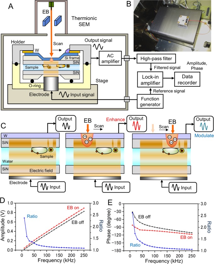
Fig 1. Experimental setup and schematic of the IP-SEM detection mechanism.
(A) Schematic of the IP-SEM system. The two SiN films enclosing the liquid sample are sealed by two sample-holding parts. The electrode under the sample holder applies the input voltage signal. The scanning-EB irradiates the upper side of the W-coated SiN film; the output signals from the W-layer are then detected by the AC current pre-amplifier and lock-in-amplifier. (B) Photograph of the sample holder setup on the AC pre-amplifier box. The sample holder was mounted on the Al stage. To detect the output signal, the upper A1 holder part is connected to the AC current pre-amplifier by a cable. (C) Schematic of the IP-SEM imaging mechanism. The input signal is applied to the bottom electrode, and the output signal from the upper W-layer is detected (left panel). When irradiated by the EB, the W-coated SiN film scatters and absorbs the electrons, modulating the SiN resistance and impedance at the EB position. The resistance modulation enhances the output signal (centre panel). When the EB irradiates the biological specimen, the output signal is attenuated by the specimen’s material (right panel). (D) and (E) Output amplitude (D) and output phase (E) of the IP-SEM system versus input frequency without sample in the holder. The EB irradiation enhances the amplitude and attenuates the phase (EB acceleration voltage 4 kV and EB current 1 nA).

