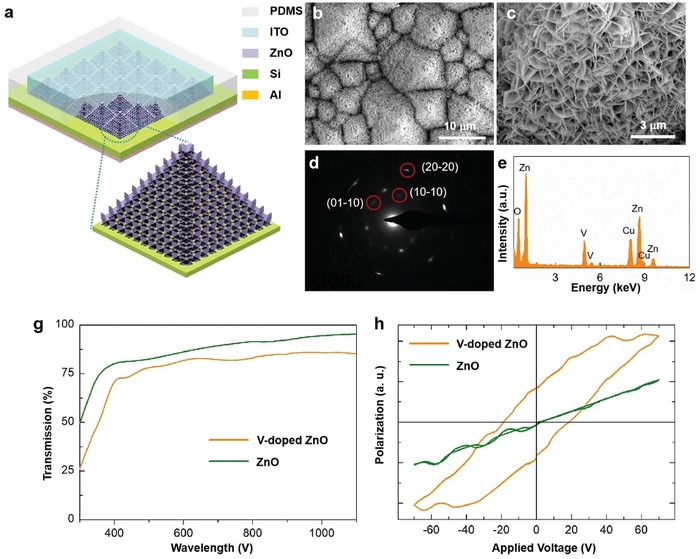
Figure 1.

Device structure and characterizations. a) Schematic structure of the FESZ‐PD. b,c) Scanning electron microscopy images of the V‐doped ZnO 2D NSs synthesized on the etched Si wafer. d) Corresponding select area electron diffraction pattern of a ZnO NS. e) Energy dispersive X‐ray spectrum of ZnO NSs. g) Transmission spectra of ZnO NSs and V‐doped ZnO NSs grown on the F‐doped tin oxide (FTO)/glass substrate. h) Polarization hysteresis loops versus electric field (P–E loops) of ZnO NSs and V‐doped ZnO NSs grown on a Cu substrate.
