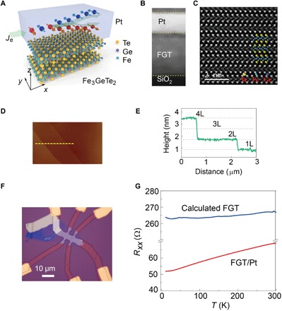
Fig. 1. Schematic view and characterizations of FGT/Pt bilayer.

(A) Schematic view of the bilayer structure. Pt layer (top) is sputtered on top of the exfoliated FGT (bottom). The green arrow represents the in-plane current flowing in the Pt layer, which generates a spin current flowing in the z direction. The accumulated spins at the bottom (top) Pt surface are indicated by the red (blue) arrows. The spin current exerts torques on the magnetization of FGT and can switch it in the presence of an in-plane magnetic field. (B) Cross-sectional STEM image of the FGT/Pt device fabricated on a Si/SiO2 substrate. The total thickness of FGT is 12.6 nm. (C) High-resolution STEM image of an FGT (87 nm)/Pt (6 nm) bilayer on a Si/SiO2 substrate. (D) Top view of the FGT exfoliated from the bulk material measured by atomic force microscopy. (E) The atomic steps profile taken along the yellow dashed lines in (D). An atomic layer step of 0.8 nm is observed. (F) The optical image of the measured Hall bar device. (G) Temperature-dependent longitudinal resistance of the FGT/Pt bilayer device and FGT only.
