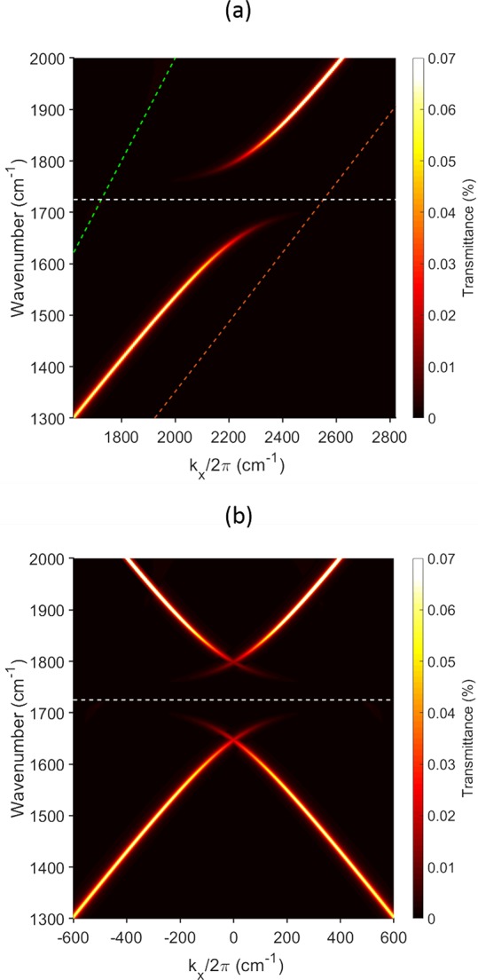
Figure 2.

Surface plasmon dispersion. Calculated dispersion of the plasmon mode associated with the gold/PMMA interface. Top (a): Calculated dispersion for a planar version (no grating) of our structures; the system comprises a silicon substrate, 100 nm of gold (the plasmon-supporting metal), a 2 μm layer of the polymer PMMA and air as the superstrate. The calculated (COMSOL) transmittance is shown as a function of frequency (cm–1) and in-plane wavevector on a color scale. High transmittance indicates a mode of the system (note that here we are considering transmittance of evanescent waves because the plasmon mode is beyond the light-line). The material parameters are given at the end of the main text. The green and red dashed lines represent the air light-line and the PMMA light-line, respectively. The horizontal white dashed line at 1732 cm–1 represents the C=O vibrational mode. Notice that the plasmon mode and the anticrossing with the molecular resonance are beyond the air light-line. Bottom (b): Here we have taken the data from (a) and superimposed a shifted and folded copy so as to produce a dispersion plot to give an idea of what we expect for a grating rather than a planar structure. The grating period was taken as 4.5 μm, for which kx/2π = 1/λg = 2222 cm–1. Here β = 0° and ϕ = 0°.
