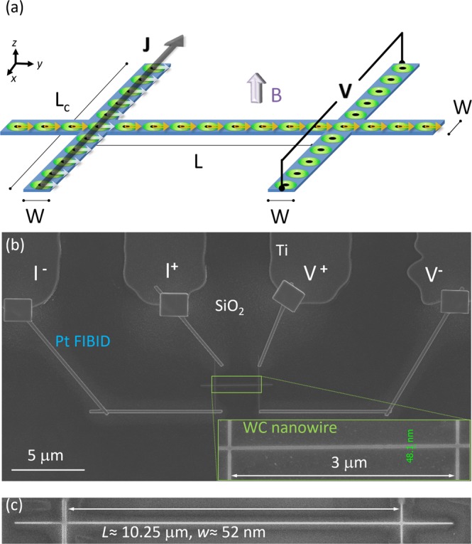
Figure 1.

(a) Overview of the sample geometry. Superconducting nanowire of width W and length L, with current and voltage contacts of length Lc and width W. Injection of the current density J occurs at the contacts on the left side, while contacts on the right side of the device are used to measure the non-local voltage V. Non-local transport of superconducting vortices occurs along the length of nanowire. Vortices are indicated by green/black circles. The Lorentz force being exerted on the vortices is indicated by white arrows. Non-local vortex motion is indicated by yellow arrows. (b) SEM image of the WC nanostructure (nanostructure A-short) for non-local electrical measurements. Inset shows a high magnification SEM image of the nanostructure A-short. (c) SEM image of the nanostructure A-long.
