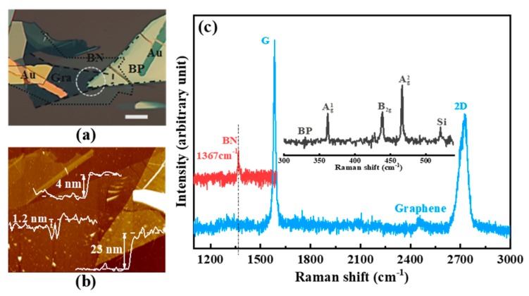
Figure 2.
(a) An optical microscope image of the black phosphorus (BP)/boron nitride (h-BN)/graphene heterojunction, where the lines indicate different materials: graphene (dashed), h-BN (point), and BP (dot-line). The scale bar is 10 µm. (b) Atomic force microscopy (AFM) images of the heterojunction device. The thickness of BP, h-BN, and graphene is ~23, ~4, and ~1.2 nm, respectively. (c) Raman spectra of exfoliated graphene (blue), h-BN (red), and BP (black) film in the device on the SiO2 substrate.

