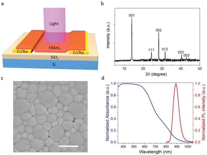
Figure 1.

Illustration of device design and material characterization for the FASnI3 PD. a) Schematic diagram of the PD. b) XRD pattern of the FASnI3 film on glass substrate. c) SEM image for the perovskite film on SiO2/Si substrate, where the scale bar is 1 µm. d) Photoluminescence and absorption spectrum of the perovskite film on glass substrate.
