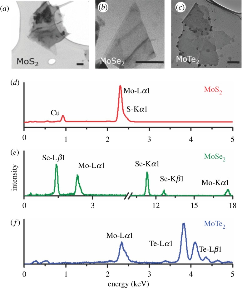
Figure 1.

TEM micrographs and EDS of the exfoliated TMD samples. Panels (a–c) are TEM images of the exfoliated TMD samples exhibiting a homogeneous multi-layered nanosheet morphology. Scale bars = 100 nm, (d) EDS of the MoS2 sample demonstrating the characteristic Mo and S peaks, along with a Cu peak from the substrate (e) EDS of the MoSe2 sample demonstrating the characteristic Mo and Se peaks, (f) EDS of the MoTe2 sample indicating characteristic Mo and Te peaks.
