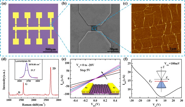
Figure 2.
(a) Optical image of graphene-based sensor arrays on the SiO2/Si substrate. (b) SEM image of an individual gas sensor device. (c) AFM image of the patterned clean graphene surface. (d) Raman spectrum of the patterned graphene channel. (e) Current–voltage (I–V) curves of the graphene-based sensors, and the inset shows the schematic illustration of the graphene FETs, where the Si substrate was used as the gate electrode. (f) Current–gate voltage (I–VG) transfer curve exhibited an ambipolar behavior with a charge neutral point near VG ≈ 5 V. The inset shows simplified band structure near the K points and Fermi level-dependent charge carrier concentration. p-type doping can create hole-like charge carriers.

