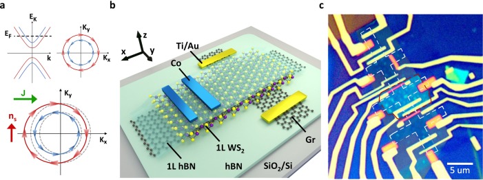
Figure 1.
(a) TMD-graphene band structure, consisting of spin-split Dirac cones with opposite spin helicity. The charge current (J) shifts the Fermi-level contours from equilibrium (gray dashed lines) and induces a nonequilibrium electron spin density (ns) by the Rashba–Edelstein effect. (b) Sketch of the van der Waals heterostructure of 1L WS2-graphene encapsulated with the top monolayer hexagonal boron nitride (hBN) and bottom bulk hBN (with a thickness of 14 nm). The device is made with Ti/Au and Co electrodes on a SiO2/doped Si substrate. The sketch illustrates the central region of the sample including the electrodes that are used for our measurements. (c) Optical microscope image of the fabricated device. The red and white dashed lines show the edges of the WS2 and etched graphene flake, respectively.

