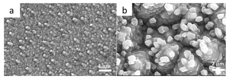
Figure 7.
SEM images of as-sputtered LCO thin films deposited (a) on polished Si substrate and (b) on textured Si substrate obtained by chemical etching. The film (b) consists of layered like grains mostly distributed as individual clusters composed of few numbers of rough grains, which were vertically agglomerated. Reproduced with permission from [75]. Copyright 2014 Elsevier.

