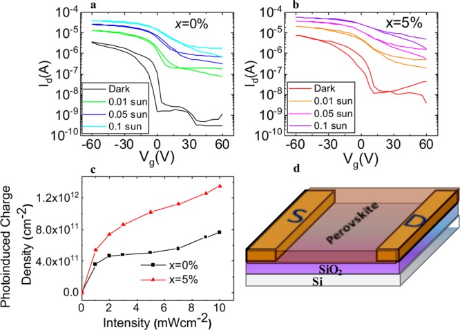
Figure 3.

Electrically gated measurements of charge transport and photoinduced doping studies on a bottom contact/bottom gate FET device (channel length 100 μm, channel width 1 mm) fabricated with x = (a) 0 and (b) 5% perovskite layers. Photoinduced characteristics correspond to white light excitation densities across the range stated. (c) Estimated photoinduced charge carrier number density in perovskite thin-film FETs. (d) Schematic of the FET architecture.
