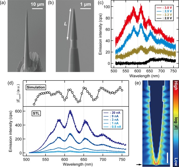
Figure 2.
STL spectra of a grooved tip. (a,b) SEM image of the FIB processed Au tip with a groove located 3 μm away from the tip apex. (c) Bias voltage dependence of STL spectra measured over the Ag(111) surface with the grooved tip (It = 1 nA, Vbias is indicated in the figure). (d) Tunneling current dependence of STL spectra measured over the Ag(111) surface with the grooved tip (Vbias = 2.5 V, It is indicated in the figure). The top panel shows the wavelength dependence of the numerically simulated electric field inside the junction 2 Å below the apex. (e) Normalized electric field distribution plotted on a logarithmic scale simulated for L = 3 μm and at 610 nm. The white lines indicate the tip shape and the black arrow indicates the position of the Ag surface. The scale bar is 500 nm.

