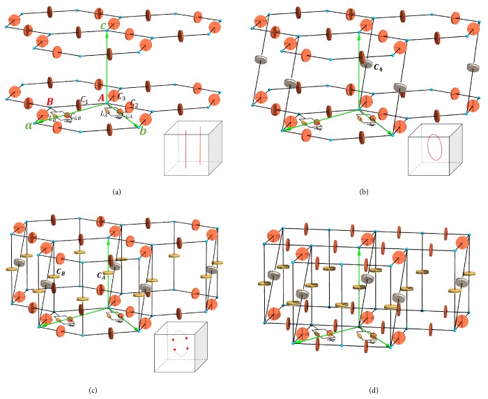
Figure 1.
Schematic setup of the three-dimensional LC circuit lattice. (a) Honeycomb layers consisting of inductors and capacitors stack along c direction without connection between each layer. The primitive unit cell consists of two inequivalent nodes A and B, which are linked by capacitors C1, C2, and C3 in the a-b plane. Each node A (B) is grounded through the parallel connected inductor LA (LB) and capacitor CGA (CGB). Lattice vectors are denoted as a, b, and c. The frequency bands structure of the single layer honeycomb LC lattice has two band-crossing points, which are uniform in kc direction and form two straight nodal lines in the BZ (red colour lines in the inset). (b) Connecting nodes A and nodes B between neighbor-layers with C4. The nodal lines become kc dependent and form a closed ring by choosing appropriate C4. (c) Connecting nodes A-A and nodes B-B between neighbor-layers with CA and CB, respectively, and removing the space inversion symmetry by tuning CA ≠ CB and CGA ≠ CGB, the nodal ring may be degenerated to Weyl points. The LC lattice can be deformed into (d), which brings convenience for constructing circuit elements in experiments with spectrum topologically invariable.

