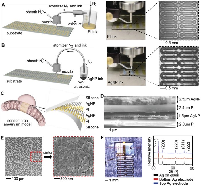
Figure 1.

AJP fabrication and material characterization. A) Illustration and image of AJP deposition of PI using a pneumatic atomizer (left). Enlarged view shows a printed PI trace (right). B) Overview of Ag deposition with an ultrasonic atomizer (left) and enlarged view of a patterned Ag on PI (right). C) Illustration of the AJP‐enabled fabrication of an implantable flow sensor in an aneurysm model. Inset shows the multilayered structure of the sensor package. D) Cross‐sectional SEM image displaying multilayered sensor structure. E) SEM images of AgNPs as printed (left) and after a sintering process, showing clusters (right). F) X‐ray diffractometer characterization of a sintered AgNPs on glass slide, bottom Ag electrode on PI, and top Ag electrode on PI. No change in crystalline structure is observed for the three cases.
