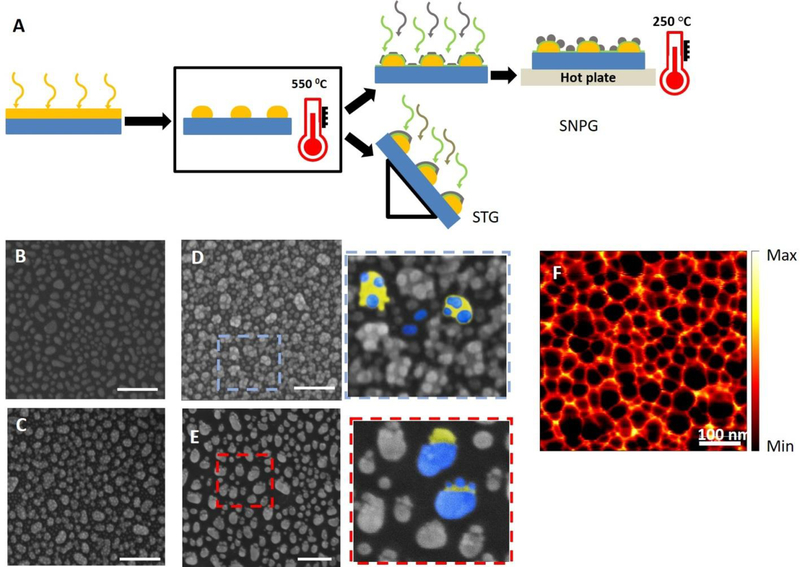
Figure 1:
Fabrication steps: (A) Scheme of fabrication, process flow from left to right. Deposition of a gold thin film (yellow) on a glass coverslip/Si wafer using electron-beam evaporation. Thermal annealing led to de-wetting of Au film and rendered the Au islands to a near-spherical shape. For SNPG configuration, 10 nm of silica (green) and 4 nm of Ag (gray) were subsequently deposited. This was followed by annealing on a hotplate to convert the Ag islands into Ag nanoparticles. For the STG samples, OAD of 10 nm of silica and 10 nm of Ag on the Au nanoparticles by placing the substrates at an oblique angle relative to the evaporant flux (87° to the horizontal). (B) Scanning Electron Micrograph (SEM) image of the Au spheres after deposition and thermal annealing. (C) SEM image of the SNPG sample with 10 nm silica and 4 nm Ag. Since the thickness of Ag film is less, the thin film is not continuous. (D) SEM image of the SNPG sample after 20 min of annealing on a hotplate. The inset shows the zoomed-in version marked by the blue dashed box. The gold (yellow) and the silver (blue) regions of the SNPG structure are highlighted in false color. (E) SEM image of the STG sample. The inset shows the zoomed-in version marked by the red dashed box. The gold (yellow) and the silver (blue) regions of the STG structure are indicated by the false color representation. The scale bars for all the SEM images marked in white are 200 nm. (F) s-SNOM image of the annealed SNPG sample; although the silver nanoparticles cannot be resolved, the gold nanoparticles are readily identified (s-SNOM image courtesy: Bruker Nano Surfaces Division).

