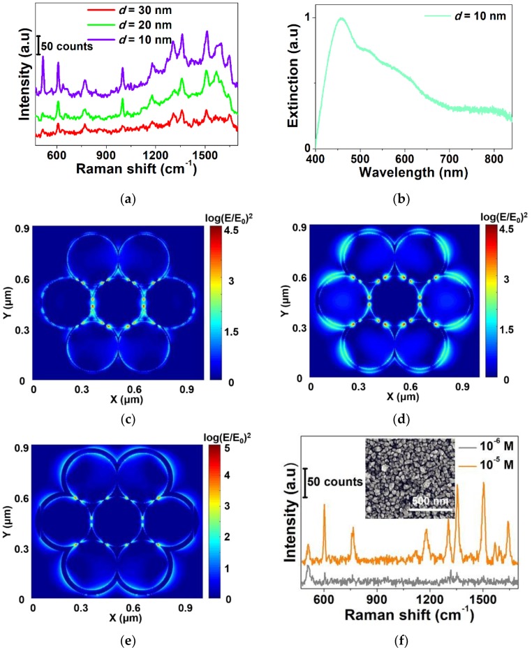
Figure 2.
(a) Raman spectra of R6G (10−9 M) deposited onto the SERS substrates with a Ag film thickness of d = 10 nm, 20 nm, and 30 nm; (b) Extinction spectrum of the SERS substrate with a Ag film thickness of d = 10 nm; (c–e) Electric field intensity distributions near the surface of the SERS substrates with an Ag film thickness of 10 nm, 20 nm, and 30 nm, respectively; (f) Raman spectra of R6G with concentrations of 10−5 M and 10−6 M deposited onto the Ag-film coated silicon wafer with a Ag film thickness of d = 10 nm. Inset is the SEM image of the Ag-film coated silicon wafer with an Ag film thickness of 10 nm.

