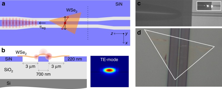
Fig. 1.
Integrated WSe2 quantum emitters. a Top view of the device: a WSe2 flake is integrated on a 220 nm thick single mode SiN waveguide, separated by 2 air trenches from the bulk SiN. The waveguide ends are tapered to allow easier coupling with a lensed fiber. The orientation of the dipole moment of the WSe2 emitters (red arrow) is random with respect to the quasi-TE polarization (approximately aligned along x−direction) of the fundamental waveguide mode (black arrow). A fraction ηwg of the total emission couples into the left-propagating waveguide mode (represented by red shaded areas). b Cross-section of the sample. The width of the air trenches and waveguide is 3 μm and 700 nm respectively. The generated PL of emitters near the waveguide couples both to free-space and to the waveguide (red shaded circles). A cross-sectional mode profile (at λ = 750 nm) of the waveguide, taken along the dotted black line in the top figure, is shown as well. c Impression of the fiber-coupled chip (inset shows light coupling from the fiber to the chip). The tapered lensed fiber is a standard SM630 fiber from Thorlabs with a focal spot size of 2 μm and an 8 μm working distance. d Microscope image of SiN chip with WSe2 transferred on waveguide region. The flake is highlighted by the white triangle

