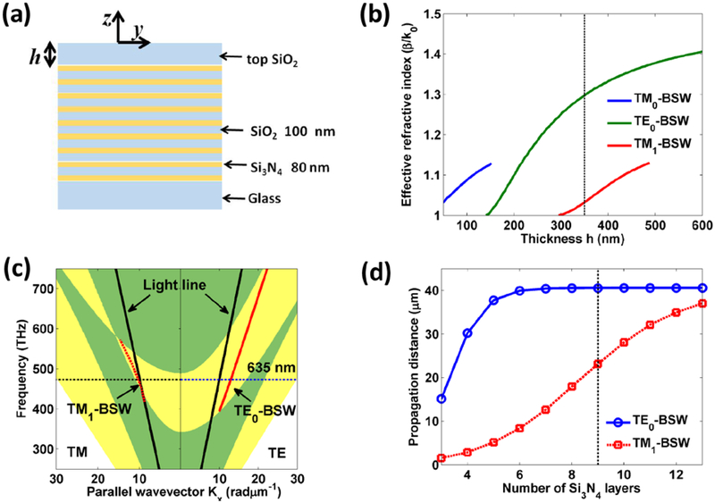
Figure 1. Photonic bandgap and BSW modes on a dielectric multilayer.
(a) Schematic illustration of the dielectric multilayer. The dielectric multilayer is made of 18 alternating dielectric layers of Si3N4 (80-nm-thick) and SiO2 (100-nm-thick). The thickness of top SiO2 layer can be varied and denoted as h. (b) the effective refractive indices of TE-BSW and TM-BSW modes versus the thickness h of top SiO2 layer. (c) The photonic band structure of the dielectric multilayer. The dispersion curves for the TE0-BSW and TM1-BSW are shown with red solid and dashed lines, respectively. The regions with yellow color denote the photonic band gap. (d) The propagation distance of TE0-BSW and TM1-BSW modes in the dielectric multilayer as a function of the number of Si3N4 layers. The thickness of the top SiO2 layer is fixed at 350 nm.

