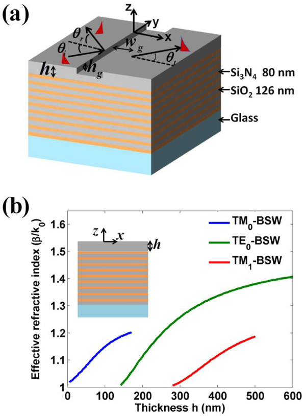
FIG. 1.
(a) Schematic illustration of the dielectric multilayer. The dielectric multilayer is consisted of 18 alternating dielectric layers of Si3N4 (80-nm-thick) and SiO2 (126-nm-thick). The thickness of top SiO2 layer can be varied and denoted as h. A groove with rectangle cross section is inscribed on the top SiO2 layer. The width and depth of groove are denoted as wg and hg, respectively. (b) the effective refractive indices of TE-BSW and TM-BSW modes versus the thickness h of top SiO2 layer.

