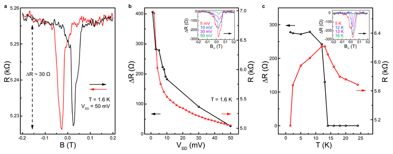
Figure 2. Bias and temperature dependent magnetoresistance measurements in device A.
a, Magnetic field dependence of the device resistance measured at T = 1.6 K. The red (black) arrow represents sweep direction from 0.2 T (-0.2 T) to –0.2 T (0.2 T). b, Source-drain bias (VSD) dependences of the change in the device resistance under the magnetic field (ΔR) and the longitudinal device resistance (R). Inset shows the resistance change under magnetic field acquired at fixed biases of VSD = 1 mV, 3 mV and 50 mV. ΔR is calculated by subtracting a polynomial fitting from the device resistance (Supplementary Information 15). c, Temperature dependence of ΔR and R. Inset shows the magnetic field dependence of the resistance change measured at T = 1.5 K, 13 K and 16 K.

