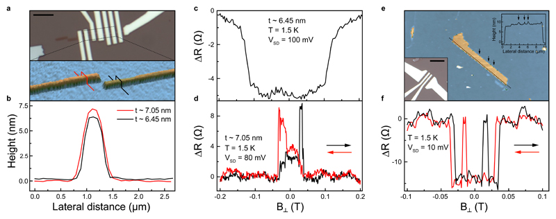
Figure 4. Layer-dependent magnetoresistance measurements.
a, Optical and AFM images of a completed PtSe2 device and its crystal, respectively. Dashed area represents the scanned AFM region. b. Cross-sectional plots along the red and black lines in a. AFM scans show that crystals used in device C and device D has one-layer difference (~ 0.6 nm) in their heights. c, Magnetic field dependence of ΔR measured from the device C (6.45 nm thick). d, Magnetic field dependence of ΔR measured from device D (~ 7.05 nm thick). e, AFM image of a PtSe2 crystal having multiple one-layer thick fragments on its surface. Top inset shows the cross-sectional plots along the black line in e. Black color arrows in e and top-inset e indicate the one-layer thick fragments. Bottom-inset e shows the optical image of the corresponding device. Black solid line represents the scale bar (5 µm) f, Magnetic field dependence of ΔR measured from the device E shown in e. We would like to note that the change in device resistance in these samples has opposite sign compared to the thinner devices shown in Fig. 2-a and Fig. S4-a. Such opposite switching signs were previously observed in Co and CoFe films.35 To determine the origin of this behavior, the effect of the number of layers, distribution of defects and their effect on magnetism need to be extensively investigated.

