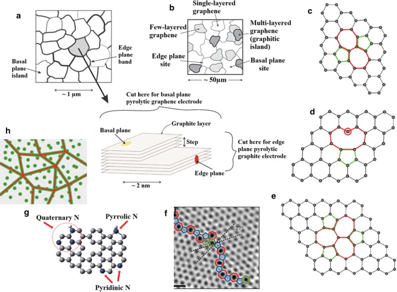
Fig. 2.
Versatility of defects in graphene. a Schematic representation of a HOPG surface showing discrete basal plane and edge plane islands. Side on view of the HOPG surface highlighting its basal plane and edge plane like-sites/defects which exhibit contrasting behaviours in terms of electrochemical activity, where electron transfer kinetics of the latter are overwhelmingly dominant over that of the former which in comparison are relatively (electrochemically) inert. Reprinted from [54] with permission of The Royal Society of Chemistry. b An underlying graphene surface with few- and multi-layered graphitic islands, indicating the basal and edge plane electron transfer sites; notice the electrode surface is akin to a HOPG surface. Reprinted from [54] with permission of The Royal Society of Chemistry. Graphene atomic structure as obtained from density functional theory (DFT) calculation for: Stone–Wales defects (c), single vacancy defect (d), and multiple vacancy defects (e) in graphene. Reprinted with permission from [146]; copyright 2010 American Chemical Society. f Aberration-corrected annular dark-field scanning transmission electron microscopy (ADF-STEM) of line defects in graphene; scale bars: 5 Å. Reprinted with permission from [147]; copyright (2010) Nature Publishing Group. g Graphene in-plane heteroatom substitution defect model: nitrogen defects. Reprinted with permission from [148]; copyright (2010) American Chemical Society. h Illustrations of a graphene sample containing both point and line defects. The red regions define the structurally damaged area (S-region), and the green circles and lines are the activated area (A-regions) where the D band is active
(Reprinted with permission from [149]; copyright 2017, IOP Publishing)

