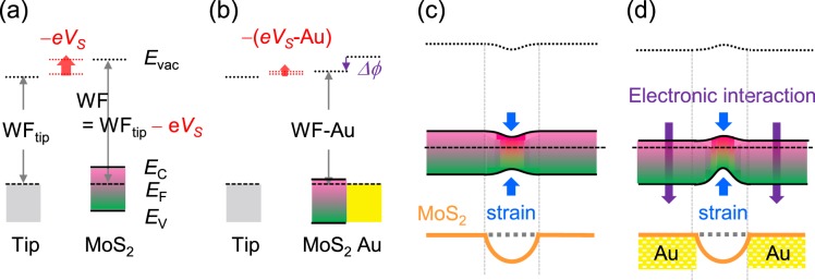
Figure 5.
(a) Schematic band diagrams to explain the relation used in KPFM measurements, WF = WFtip − eVS, where WF, WFtip, e, and VS are the work function of a sample (MoS2), the work function of the tip, the electron charge, and the surface potential, respectively. Evac, EC, EF, and EV are the vacuum level, conduction band minimum, Fermi level, and the valence band minimum of a sample, respectively. (b) The interfacial electric dipole energy, Δϕ, lowers the WF of the MoS2 region on the Au stripe (WF-S). It should be noted that eVS = WFtip − WF. The band diagrams in (a,b) indicate VS < 0, consistent with our experimental results. Thus, reduction of WF increases VS and decreases |VS| (VS < 0), as illustrated in (b). Schematic band diagrams and illustration of the MoS2 monolayers on the Au stripe arrays in the dark, when including (c) only strain-induced bandgap reduction and (d) additional electronic interaction at the MoS2/Au interface.

