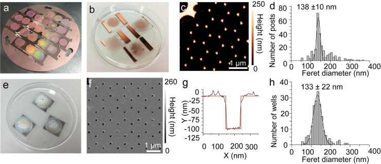
Fig 3. AFM characterization of Al devices.
(a) Structural coloration from the bead diffraction pattern following Cu evaporation. (b) Coverslips with centers patterned by arrays of copper posts following dissolution of polystyrene beads by toluene and tape pull of copper that had coated the tops of the beads. (c) AFM image of Cu posts on coverslip. (d) Distribution of apparent maxFeret diameter at half-maximum height of posts formed using a bead template annealed for 20 s. (e) Completed Al ZMWs. (f) AFM of ZMW wells formed after dissolving the narrow Cu posts. (g) AFM profile of depth of individual well. (h) Distribution of apparent maxFeret diameters of wells in Al ZMW measured at half-maximum depth.

