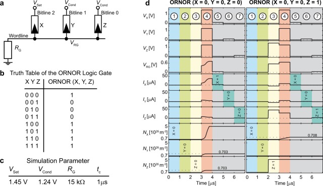
Figure 1.
The ORNOR gate’s (a) structure and (b) truth table. (c) Simulation parameter for the circuit of (a). (d) The simulation of the critical cases of the ORNOR gate are depicted. Here, the subscripts X, Y, Z are indicating the correlation of the applied voltages, currents or state variables to the devices X, Y and Z, respectively. In step 1–3 the initialization process of the ORNOR gate is shown by writing the three inputs to the devices X (blue), Y (light green) and Z (yellow). In step 4 (red) the ORNOR operation is executed, which is followed by three verifying read-out steps (dark green). If a high current is detected the read-out value is a 1, whereas a low current is a 0. Row 1/2/3: voltage applied to the Bitline 2/Bitline 1/Bitline 0. Row 4: potential at the wordline. Row 5/6/7: current at Bitline 2/Bitline 1/Bitline 0. Row 8/9/10: state variable of device X/Y/Z. The scale is changed for small state variable values.

