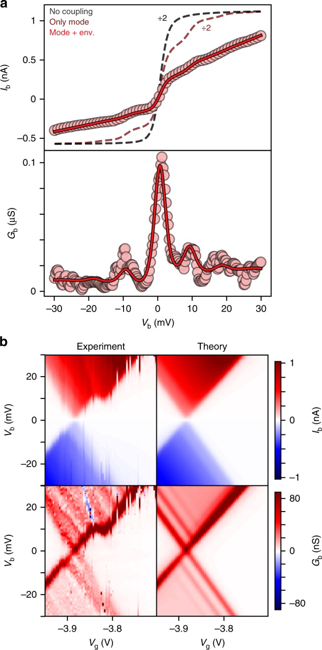
Fig. 2.

The contributions of inner and outer sphere vibrational interactions in device A. a Current (Ib) and differential conductance (Gb) as a function of bias voltage (Vb) of device A (circles) at 5 K, corresponding fit to our model (red line), and corresponding curves without environmental coupling (dark red line) or without vibrational coupling (black line). b Experimental current (left top) and differential conductance (left bottom) maps as a function of bias and gate voltage of device A, and reconstructed maps (right) from the parameters used to fit the IV trace in a). At higher (positive) bias we observe switching in the stability diagram most likely resulting from a nearby charge trap30. This effect is however inconsequential to the phenomena discussed here
