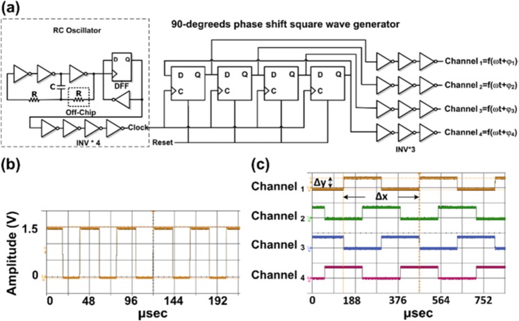
Figure 3.
The travelling-wave built-in driving circuit. (a) The schematic architecture of implemented travelling-wave built-in driving circuit. (b) The tuned clock frequency of built-in ring oscillator clock is operated at 24.08 kHz. (c) The experimental output of 90-degreeds phase shift waveform measured under designed clock frequency. Δx and Δy are represented a period and amplitude of the output frequency of channel 1 with phase term is 0°, 1/Δx is measured as 2.985 kHz and Δy is the 1.5 V peak to peak voltage of the on-chip circuit driving output.

