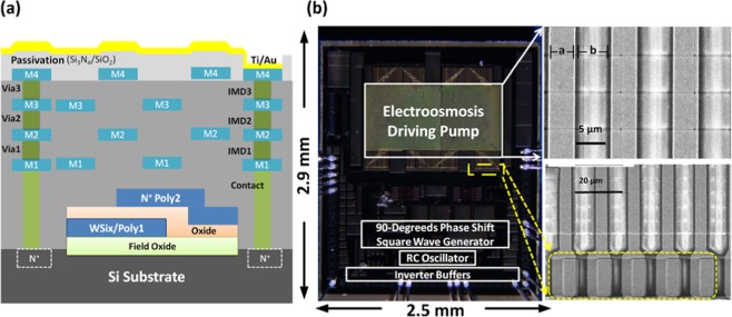
Figure 5.
(a) The schematic diagram of the contents layers of 0.35 μm CMOS Bio-MEMS process. In this schematic, metal layers (M1-M4) are the layers for electronic circuit layout routing, Via1-Via3 are the interconnection between adjacent metal layers, and inter-metal dielectric layers (IMD1-IMD3) are the dielectric layers used to electrically insulate interconnect lines. (b) The images of the fabricated chip and the SEM picture of the fabricated electrodes and interconnections array. The yellow dash square represents the double –size width designed of contact points between Ti/Au and M4 layers.

