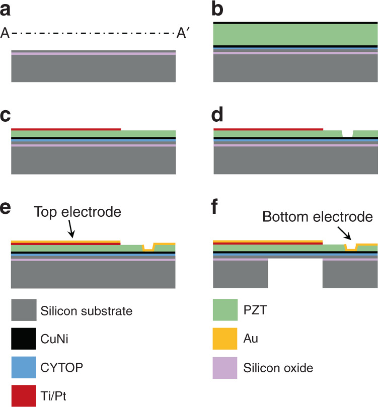
Fig. 2. Fabrication process of the pMUT array (section A–A’ in Fig. 1b).

a A 4-inch silicon-on-insulator (SOI) wafer with 15 μm of top silicon was prepared; b the SOI wafer was bonded with a bulk PZT using CYTOP as a bonding layer; c the PZT film was thinned using a chemical mechanical polishing (CMP) process; the Ti/Pt layers were deposited and patterned on top of the PZT layer; d the PZT layer was etched to form a hole for the bottom electrode; e an Au layer was deposited and patterned to form the top and bottom electrodes; f the membrane was released from the backside through the DRIE process
