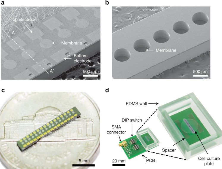
Fig. 3. Images of the fabricated pMUT array and packaged device.
a SEM image of the bottom view of the fabricated pMUT array showing section line (A–A’) of Fig. 2; b SEM image of the top view of the fabricated pMUT array; c optical image of the fabricated pMUT array; d optical image of the packaged device with the pMUT array, showing the DIP switches soldered on the PCB to control individual transducers and spacers to maintain a constant distance between the cell culture plate and the transducers; voltage was applied to the pMUT array through an SMA connector

