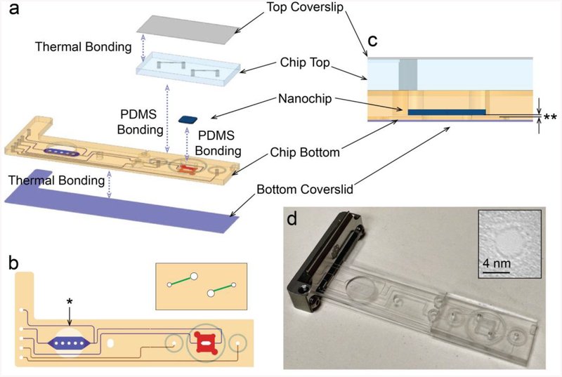
Figure 1.
a) A schematic diagram of the microfluidic chip assembly. b) Top view design. The channels leading to/from the sample preparation chamber and to/from the bottom of the nanopore device are labeled blue, the channels leading to/from the top of the nanopore chamber are labeled in red. The blue and red channels are both cut into the bottom half of the two part device. The top half of the device is shown above and connects the four through hole channels fed by the red channels on the bottom of the device up through the Zeonex plastic to access the top of the nanopore chamber and the green channels. Both the red and blue channels flow past fluidically separated embedded electrodes. The bottom half of the device has the channels (red/blue) micro-machined on the bottom of the thick Zeonex plastic and sealed with a cover slip to form a channel while the top of this half has a feature micro-machined for the magnet holder (noted by asterisk). The top half is sealed with PDMS glue to the bottom half using the 3 micromachined tracks in the top of the bottom half as a guide. c) Zoom in cross section of the chip at the nanopore chambers. Noted that the chip bottom is machined from both top and bottom side, creating the thinnest layer of ~200 microns (labelled as **). d) A photograph of the microfluidic chip in its assembled state. Inset is the transmission electron micrograph of the nanopore taken after drilling.

