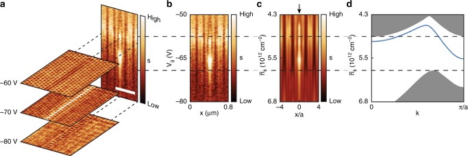
Fig. 3.
Gate dependence of the 1D plasmonic domain wall state. a Stacked near-field images (analogous to Fig. 2c) and detailed voltage-dependent contrast across the artificial domain wall (vertical panel) collected at ω = 904 cm−1. Scale bar: 400 nm. b The same data as panel a vertical panel, displayed in 2D false color map of near-field signal s as a function of gate voltages Vg and position x across the domain wall. c Simulated voltage-dependent measurement based on point dipole model. is the averaged carrier density. The position of the domain wall is marked by an arrow. The lattice periodicity a = 80 nm. d 1D plasmonic dispersion simulation for the structure shown in Fig. 2a. Gray region corresponds to 2D plasmonic modes. The blue solid line highlights the 1D domain wall state

