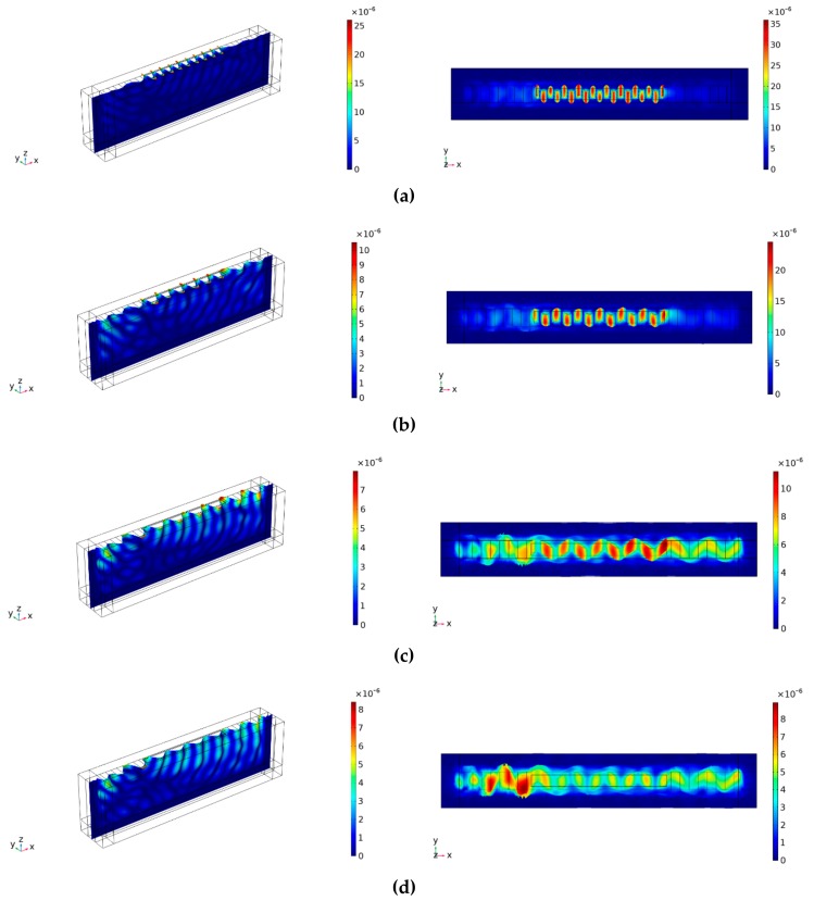
Figure 7.
Snapshots of sectional views on a Y + 36° cut substrate with different thicknesses and materials (first column spatial displacement, second column displacement along the Y-direction) (a) 0.03 λ-thick gold wave-guide layer at 455 MHz; (b) 0.025 λ-thick platinum wave-guide layer at 421 MHz; (c) 0.035 λ-thick titanium wave-guide layer at 438 MHz; and (d) 0.03λ-thick silicon dioxide wave-guide layer at 449 MHz.

