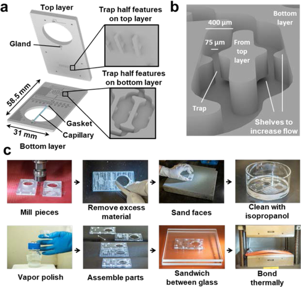
Figure 3 |. Scalable manufacturing of the Islet on a Chip.
a. Exploded view of the islet chip drawing in Figure 1b to show integration of the glass capillary and trap features on each layer before bonding. b. Angled, zoomed view of two adjacent islet traps in the islet chip drawing in Figure 1b to visualize channel and trap detail. Middle island between each pair of channels protrudes from the bottom surface of the top layer and fits into the channel to complete the trap during bonding. A small opening above or below each wall in the traps was designed to increase flow through the traps. c. Photographs of steps in chip fabrication. First, chip features are milled into polycarbonate and excess material is removed. Layers are then sanded, cleaned, and vapor polished. Finally, the capillary is assembled between polished layers and bonded together.

