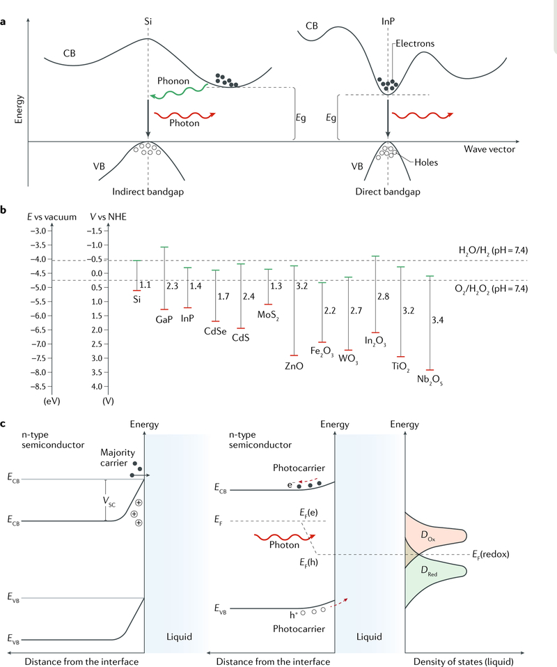
Fig. 2 |. Material physics at the semiconductor-saline interface.
a | Band structures of inorganic semiconductors. The bandgap Eg is defined as the energy difference between the lowest point of the conduction band (CB) and the highest point of the valence band (VB). A semiconductor can have either an indirect or a direct bandgap. In an indirect bandgap semiconductor (for example, Si), the VB and CB edges are not aligned in the momentum space and thus the electrons in the VB cannot be directly excited to the CB without the assistance of phonons. In a direct bandgap semiconductor (for example, InP), the electron transfer between the VB and the CB occurs directly through the absorption or emission of photons. The two band structures are not to scale. b | Band edge positions of different inorganic semiconductors with respect to vacuum level and normal hydrogen electrode (NHE) potential. The redox potentials of the H2O/H2 and O2/H2O2 couples at physiological pH are drawn as references (dashed lines). Band edge positions and bandgap energies are based on data from the literature83,97,216–219. c | Band bending at semiconductor-saline interfaces. Band bending occurs if a semiconductor is immersed in a saline solution, as the charge flow between the solid and liquid phases aims to reach an equilibrium in terms of Fermi levels (EF = EF(redox)). ECB and EVB are the energies of the CB and VB edges, respectively. VSC is the semiconductor barrier height at the depletion layer. Illumination of the semiconductor causes different energy distributions of the photogenerated carriers (that is, electrons and holes (h+)) occupying the corresponding quasi-Fermi levels EF(e) and EF(h). Swept by the built-in electric field, photocarriers can be injected into the solution for surface electrochemical reactions with the corresponding redox species. DOx and DRed are the densities of states for oxidants and reductants in the saline solution, respectively.

