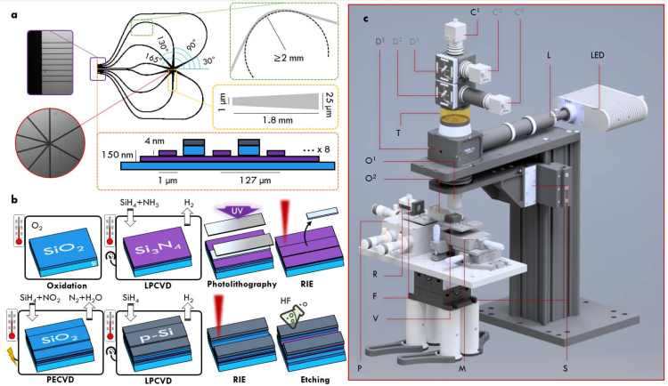
Fig. 2.
(a) Chip design: 8 inputs deliver visible light at various illumination angles to the imaging region, while simultaneously ensuring single-mode characteristics through bending (bend radii ≥ 2 mm) and adiabatic tapering. (b) Waveguide production steps: the surface of a silicon waver is thermally oxidized and subsequently covered with a layer of silicon nitride via low-pressure chemical vapor deposition (LPCVD). The waveguides structure is then created via photolithography and reactive ion etching (RIE) to produce the required 4 nm-sized rib. A protective wall between the waveguides is created via plasma-enhanced CVD of silicon oxide followed by LPCVD of polycrystalline silicon. RIE followed by chemical etching using hydrofluoric acid (HF) uncovers the waveguides again [15]. (c) The optical microscope as outlined in the main text: LED illuminator (LED), liquid light guide (L), fibre input for lasers (F), reflective collimator (R), vacuum stage (V), piezo stage (P), micrometer stage (M), sample stage (S), objectives (O1/2), tube lens (T), (dichroic) mirrors (D1/2/3), cameras (C1/2/3).

