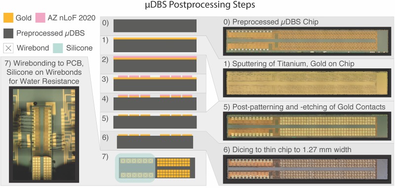
FIGURE 3.
Design architecture for μDBS post-processing. Fabricated chips (0) undergo gold deposition (1) and are covered with AZ nLoF 2020 negative photoresist (2). Photoresist is exposed to UV light according to the desired contact layout through a photolithography mask and regions of photoresist not exposed to light are removed (3). Gold and titanium layers are etched away from regions not covered by photoresist to define the gold contacts (4). Remaining photoresist is washed off (5) and the chips are diced to the appropriate size (6). Connection pads are wirebonded to test PCBs (7) to enable device programming and functionality testing. Silicone was used to insulate non-contact regions from water exposure during the validation experiments.

