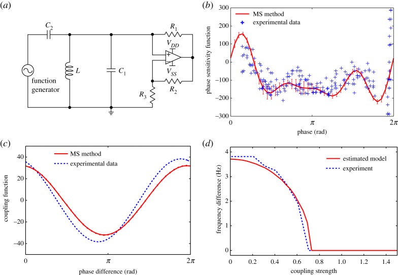
Figure 5.
Experiment of Van der Pol oscillator circuit. (a) Schematic illustration of the Van der Pol circuit, that is composed of an inductor (L), a capacitor (C1), three resistors (R1, R2, R3), an operational amplifier, and its associated power supplies (VDD, VSS). External forcing is injected from a function generator (Keysight 33500B) through a capacitor (C2). (b) Phase sensitivity function estimated by the multiple-shooting method (red line) and the perturbation experiment (crosses). (c) Coupling functions estimated by the present method (solid red line) and one (dashed blue line) obtained by the averaging of the experimentally obtained phase sensitivity function and the sinusoidal input waveform. (d) Synchronization diagram of the estimated phase model (solid red line) and the experimental circuit system (dashed blue line). (Online version in colour.)

