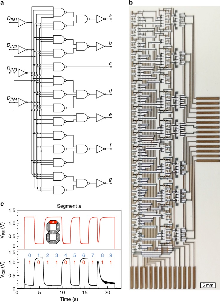
Fig. 4.
Binary-coded decimal 4-to-7 decoder. a Schematics of a 4-to-7 decoder implemented with inverters and NAND gates, including two-, three-, and four-input NAND gates. b Photograph of the all-printed decoder that consists of 87 PEDOT:PSS-based OECTs (scale bar: 5 mm). Note that the details of the seven rightmost sub-circuits, representing the display driver circuitry including 28 additional OECTs, are omitted in this discussion. Four of the 14 pads located in the lower part of the image are input signals (DIN1, DIN2, DIN3, DIN4), whereas the other pads are dedicated to VDD, VSS, two GND pads, pixel voltage, enable signal, and four pads for testing. Each display segment (a, b, c, d, e, f, g) consists of one pixel electrode and one counter electrode, which results in seven pairs of output pads located on the right side of the image. These output pads are used for circuit characterization, or to connect the circuit with an external display device. c Logic voltage output sequence (VPE, data shown in red are the logic level controlling the display pixel electrode) of segment a [1,0,1,1,0,1,0,1,1,1] when the input signal corresponds to the digits [0,1,2,3,4,5,6,7,8,9]. The data shown in black are the logic voltage level controlling the display counter electrode (VCE), hence, the two data sets are inverse to each other. The input signal representing the counting sequence from 0 to 9 is provided by changing the input signals DIN1 to DIN4, e.g. [0,0,0,0], [0,0,0,1], [0,0,1,0], etc., every two seconds. The glitch at ~18 s is owing to the fact that the switching time varies between different OECTs within the circuit

