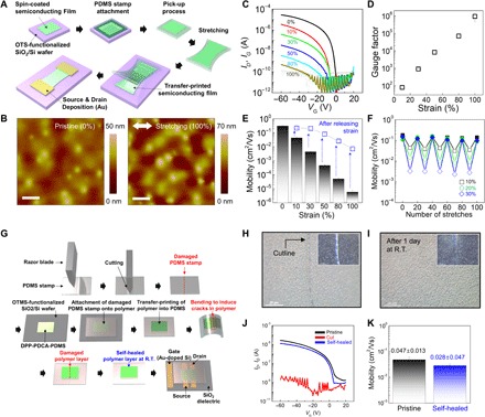
Fig. 2. Strain-sensitive property of self-healable semiconducting film.

(A) Schematic illustration for sequential fabrication procedures of the OTFT with stretchable self-healable semiconducting film (200 nm) using transfer-printing assembly. (B) AFM height images for pristine and stretched (100%) semiconducting films. Scale bars, 1 μm. (C) Transfer curves of OTFTs as a function of strain applied to semiconducting film along the tensile stretching direction and (D) GFs extracted from on-current of OTFTs. (E) Field-effect mobilities on strain and after releasing strain measured for the same device. (F) Field-effect motility as a function of stretching cycle at different strains. (G) Schematics for fabrication methods of the self-healed semiconducting film that was cut by bending a partially cracked PDMS stamp and its OTFT. (H) Optical microscope (OM) images of damaged semiconducting film through self-healing process and (I) self-healed film. Inset: Corresponding dark-field OM images. (J) Transfer curves and (K) field-effect mobility of pristine and autonomously healed OTFTs. R.T., room temperature.
