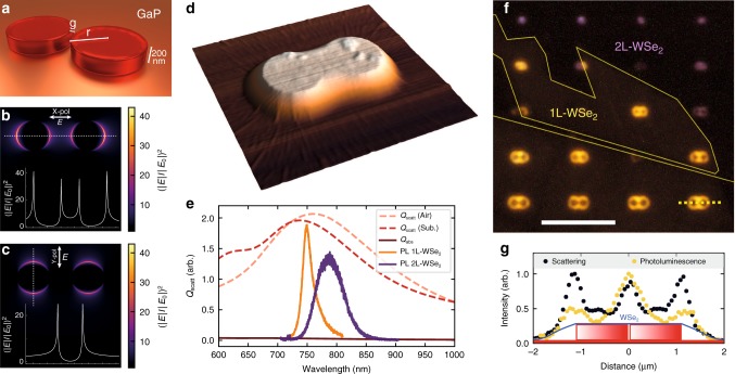
Fig. 1.
Coupling of an atomically thin semiconductor to a dielectric nano-antenna. a Schematic view of a GaP dimer nano-antenna with a height = 200 nm, gap width g, and pillar radius r. b, c Calculated relative intensity of light at 685 nm scattered by a GaP dimer with = 50 nm, = 200 nm, and = 65 nm. () is the electric field amplitude of the light scattered by (normally incident on) the dimer. The polarisation of the incident light is shown with arrows. is calculated at the height of 200 nm corresponding to the top surface of the pillars. The inset shows the variation of along the horizontal and vertical dotted lines. d Atomic force microscopic (AFM) image of a GaP nano-antenna ( nm) covered with a monolayer WSe. e Simulated scattering () and absorption () efficiency integrated over numerical aperture NA = 0.9 for a GaP nano-antenna ( = 35 nm, = 100 nm) illuminated with a plane wave. Pink (red) dashed line for light scattered upwards in air (downwards into the substrate). Room temperature PL spectra are shown for 1L-WSe (orange) and 2L-WSe (purple). f Optical microscopic image showing PL from dimer nano-antennas array covered with 1L- and 2L-WSe illuminated with unpolarised white light (see ‘Methods’ for details). Scale bar is 10 μm. The yellow lines show the boundaries between 1L- and 2L-WSe. PL from 1L (2L) sample shows as false yellow (purple) in the image. g Intensity profiles extracted from a dark-field (black) and PL (yellow) microscopic images for a dimer with = 500 nm measured along the dashed line in e. The intensity profiles are overlaid with the schematic of a dimer

