
Fig. 3. Effect of PEDOT lattice parameter on electrical conductivity.
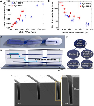
(A) b-axis lattice parameter as a function of OSR in PEDOT films grown at the different deposition temperature of 110° and 140°C. (B) The relation of electrical conductivity and b-axis lattice parameter of PEDOT films grown at the different deposition temperature. (C) Schematic illustrations of possible current transport direction in the pure face-on orientation with low-angle grain boundaries. (D) Illustration of the high impact of low b-axis lattice parameter (short π-π stacking distance) and chain bridging to avoid localization in the pure face-on microstructure. The blue arrows display the direction of current flow. (E) Schematic illustration of b-axis lattice parameter influence on the intra- and interchain charge transport. The intrachain charge transfer was affected by the doping level, while the interchain charge transfer was influenced by the charge transfer integral. (F) Left: The cross-sectional scanning electron microscopy (SEM) image of the oCVD PEDOT film grown by VOCl3 as an oxidant with a thickness of ~80 nm on a silicon wafer with etched trench structures demonstrating high conformality of the deposition. Right: The cross-sectional SEM image of the highly conformal oCVD PEDOT film on a trench with high magnification.